Major: COMPUTER HARDWARE
High Speed SRAM design methodologies and It's application to Cache memory
| 1983/March | BS degree from Osaka Univ. Electronic Engineering, JAPAN | |
| 1992/January | MS degree from Stanford Univ.
Electrical Engineering, USA Major: COMPUTER HARDWARE |
|
| 1994/December | PhD from Osaka University, JAPAN High Speed SRAM design methodologies and It's application to Cache memory |
| 1983/4-1990/7 | Designer at Mitsubishi
Electric LSI research Laboratories
|
| 1990/7-1992/1 | Stanford University
Electrical Engineering Master course
|
| 1992/1-1995/12 | Cache design project
leader in Mitsubishi Electric for INTEL corporation
|
| 1995/1-1996/5 | Design member for 3D
rendering ASIC jointly developed by Mitsubishi Electric
& Evans&Sutherland, UTAH
|
| 1996/6-1997/7 | Design member for Flash
memory
Design member for low voltage SRAM (mobile application)
|
| 1997/7-1999/4 | 300MHz pipelined burst
cache SRAM design team leader, presented at ISSCC99 Å@ |
| 1999/5 | Associate Professor at the University of the Ryukyus, System on chip design |
| 2001/4 | Professor at the University of the Ryukyus |
| 1997/4-1999/3 | IEEE International Solid-State Circuit Conference Far East Committee Member |
| 2004/4- | Asia pacific-DAC University LSI Design Contest Committee Member |
| 2001/1- | Japan Society of Promotion Science, 165(VLSI)-Committee Member |
| 2002/4-2003/3 | Asia pacific-DAC University LSI Design Contest Chairman |
| 2001/3- | Magna Design Net, Inc Chief Scientist |
| 2002/4- | Co-Professor at the Japan Advanced Institute of Technology |
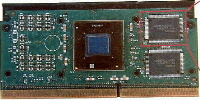 Pentium!!!Å@Å@
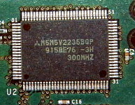 300MHz Cache