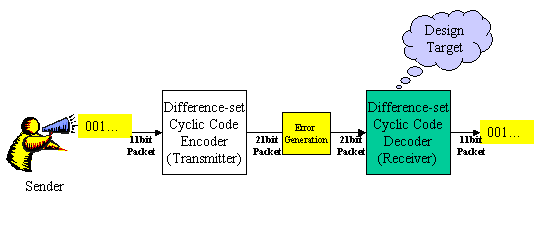
Figure1 System Diagram
Tom Wada, Prof of the University of the Ryukyus, Information Engineering Dept.
This year's design task is the Digital Error Correction Circuit, which is used for Character broadcasting stream in Japan Television broadcasting system. Since this contest is mainly for University students, the code size in the task is relatively small to let student to design easily. In addition, some task level is prepared for several students levels.
The requirements of the design is to write HDL (VHDL or Verilog HDL) and to synthesize digital circuits using Synopsys design analyzer or any other EDA tools. Making FPGA is also optional but our judges love to see your FPGA designs.
Figure1 System Diagram
The figure 1 shows the diagram of the design task. It is divided into Transmitter and Receiver. What you have to design is the Receiver. The sender generates serial bits. The transmitter takes 11 bits from the sender and add more parity 10 bits using the Differential Cyclic Coding. Then the transmitter makes 21 bit packets. In the real communication, bit error happens by some noises. In the figure 1, Error Generation block generates this random bit error.
The Receiver gets the 21 bit data packed with error and perform the error correction processing. Reed-Solomon error correction is very famous method. But it's circuit size is large then it is not good task for students. The Differential Cyclic Code needs small hardware size then it is good difficulty level for this contest.
One famous method to identify bit errors in digital communication is parity checking. The table 1 shows one example of parity check. One parity bit is generated for 8 bit data. The one parity bit is '1' when there are even number of '1's in the data and the parity bit is '0' when there are odd number of '1's in the data. Then the parity bit generation login is simply exclusive-or of the 8 data bits.
|
8 data bits |
1 parity bit | parity bit generator (exor) | |||||||
| D7 | D6 | D5 | D4 | D3 | D2 | D1 | D0 | Parity | 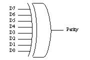 |
| 1 | 0 | 1 | 1 | 0 | 0 | 0 | 1 | 0 | |
| 0 | 0 | 0 | 0 | 0 | 0 | 0 | 0 | 0 | |
| 0 | 1 | 0 | 0 | 0 | 0 | 0 | 0 | 1 | |
Table1: 8 bit parity and generator
Then, the 9 bits, which is the data and the parity, is transmitted and the exclusive-or of the 9 bits {D7, D6, D5, D4, D3, D2, D1, D0, Parity} will be '0' when error doesn't happen in the transfer. If the exclusive-or of the 9 bits is '1', we can detect there is error in the data transfer. However, the error can not be corrected. What we can know only is the detection of the error.
First, I try to explain the mechanism of the Differential Cyclic Code Error correction without explaining complicated Galois fields mathematics. The target system in this design task has 11 information bits and 10 parity bits. The one transmission packet size is 21 bits. This 21 bits has the following characteristics. The table 2 show the example when the information bits are all '1's. The corresponding parity bits are shown in the table, too.
|
parity bits (10 bits) |
information bits (11 bits) |
||||||||||||||||||||
| Information 11 bits | 1 | 1 | 1 | 1 | 1 | 1 | 1 | 1 | 1 | 1 | 1 | ||||||||||
| Transmission packet 21 bits | 0 | 0 | 1 | 1 | 0 | 0 | 1 | 0 | 0 | 0 | 1 | 1 | 1 | 1 | 1 | 1 | 1 | 1 | 1 | 1 | 1 |
Table 2: one example of 11 information bits and 21 bits transmission packet
Let's take a look at the following five parity check.
| The position of the bits | 0 | 1 | 2 | 3 | 4 | 5 | 6 | 7 | 8 | 9 | 10 | 11 | 12 | 13 | 14 | 15 | 16 | 17 | 18 | 19 | 20 |
| Transmission packet (SB) | 0 | 0 | 1 | 1 | 0 | 0 | 1 | 0 | 0 | 0 | 1 | 1 | 1 | 1 | 1 | 1 | 1 | 1 | 1 | 1 | 1 |
| parity check A1 | 1 | 1 | 1 | 1 | 1 | ||||||||||||||||
| parity check A2 | 1 | 1 | 1 | 1 | 1 | ||||||||||||||||
| parity check A3 | 1 | 1 | 1 | 1 | 1 | ||||||||||||||||
| parity check A4 | 1 | 1 | 1 | 1 | 1 | ||||||||||||||||
| parity check A5 | 1 | 1 | 1 | 1 | 1 |
Table 3: The five parity checks position
In the table 3, the parity check A1 has indicator '1's at the positions of 9, 12, 13, 18, 20. The corresponding transmission packet bits are SB(9), SB(12), SB(13), SB(18), SB(20). If we take the parity check of those bits, that is, exclusive-or (EXOR); the result is '0'. Please see the table 4. For other four parity checks, all exor outputs are '0's.
| parity check A1 | A1 = SB(9) exor SB(12) exor SB(13) exor SB(18) exor SB(20) = 0 |
| parity check A2 | A2 = SB(1) exor SB(11) exor SB(14) exor SB(15) exor SB(20) = 0 |
| parity check A3 | A3 = SB(4) exor SB(6) exor SB(16) exor SB(19) exor SB(20) = 0 |
| parity check A4 | A4 = SB(0) exor SB(5) exor SB(7) exor SB(17) exor SB(20) = 0 |
| parity check A5 | A5 = SB(2) exor SB(3) exor SB(8) exor SB(10) exor SB(20) = 0 |
Table 4: The five parity check equations
Assume the case that the 20th bits SB(20) has error. The SB(20) is included in all the five parity check equations. Then, those five parity check bits are all '1's.
Assume another case that 1bit error happens at the position of the transmission packets other than SB(20). As you see in the table 3, the 1 bit error position other than SB(20) is just included in only one equation. Then only one parity check equation will be '1'. The other four parity check equations are all '0's.
Then, if you compute the five parity check equations and only if you find plural results are '1's, you can detect the error.
I have shown the error correction of SB(20) in the previous section. In this section, errors in other positions will be explained.
| The position of the bits | 0 | 1 | 2 | 3 | 4 | 5 | 6 | 7 | 8 | 9 | 10 | 11 | 12 | 13 | 14 | 15 | 16 | 17 | 18 | 19 | 20 |
| Transmission packet (SB) | 0 | 0 | 1 | 1 | 0 | 0 | 1 | 0 | 0 | 0 | 1 | 1 | 1 | 1 | 1 | 1 | 1 | 1 | 1 | 1 | 1 |
| parity check A1 | 1 | 1 | 1 | 1 | 1 | ||||||||||||||||
| parity check A2 | 1 | 1 | 1 | 1 | 1 | ||||||||||||||||
| parity check A3 | 1 | 1 | 1 | 1 | 1 | ||||||||||||||||
| parity check A4 | 1 | 1 | 1 | 1 | 1 | ||||||||||||||||
| parity check A5 | 1 | 1 | 1 | 1 | 1 |
Table 5: Parity check method for correcting SB(19)
In the table 5, the parity check method for SB(19) correction is shown. The table is simply shifted to the right-hand side. The overflow at the most right-hand side is fed into the most left-hand side. As you can see in the table 5, you can correct SB(19) using the same method.
When you repeatedly shift the table, you can correct any bits in the transmission packet.
From now on, inevitably I have to explain this system using Galois fields polynomials.
Assume the 11 information bits are {u0, u1, u2, u3, u4, u5, u6, u7, u8, u9, u10}. Then we can make the polynomial for the information bits as U(x).
![]() ---- (1)
---- (1)
The power of x indicates the position of the bits.
The we can make the polynomial SB(x) for the transmission packet.
 ----(2)
The table 6 summarize the all coefficients in the polynomials.
|
10 parity bits |
11 information bits |
||||||||||||||||||||
| Information bits | u0 | u1 | u2 | u3 | u4 | u5 | u6 | u7 | u8 | u9 | u10 | ||||||||||
| Transmission packet | r0 | r1 | r2 | r3 | r4 | r5 | r6 | r7 | r8 | r9 | u0 | u1 | u2 | u3 | u4 | u5 | u6 | u7 | u8 | u9 | u10 |
Table 6: Coefficients of information equation U(x) and transmission packet equation SB(x)
Accordingly, If we can find
![]() ----(3) ,
----(3) ,
we can easily make SB(x) since we know U(x).
The R(x) is can be solved X(x) divided by G(x) since R(x) is the remaining.
![]() ----(4)
----(4)
![]() ----(5)
----(5)
However, this calculation have to be in Galois Fields. The rank of the equation (5) is 10. Then the rank of equation (3) is less than 9.
Actually to get the remaining is simple.
![]() ----(6)
----(6)
Using the equation (6), we can transfer a equation of more than rank 10 into the equation less than rank 7. Be sure to remember that the addition and subtraction all become EXOR as the following examples.
 ----(7)
Figure 2 show the circuit diagram of the transmitter. Synchronizing the system Clock, information bits u10, u9, ..., u0 are input to the circuit thru the node IN in this order while the two switches are connected to the node A. Then the same information bits u10, u9, ..., u0 appears the node OUT. At the same time, the circuit calculate R(x). Since the X(x) is divided by
![]() ----(5) ,
----(5) ,
We can use the
![]() ----(6)
----(6)
to reduce the rank of the equation. If you carefully take a look at the circuit, you can see the function of equation (6). As a result, when all 11 information bits are entered, 10 flip-flops r9, r8, ..., r0 will posses the reminder. Then the two switches are connected to B and the reminders r9, r8, ..., r0 are sequentially be output to the node OUT. The detail timing diagram of the operation is shown in the figure 3.
![]()
Figure 2: Circuit of the transmitter
![]()
Figure 3: Timing Diagram of the transmitter
In figure 3, the START signal is used to indicate the start timing. In addition, using the START signal, all r9, r8, ..., r0 flip-flops are synchronously reset.
In the table 8 and 9, the flip-flop values are shown to help your understanding. The table 8 for the information is (0,0,0,0,0,0,0,0,0,0,1) and the table 9 is for (1,1,1,1,1,1,1,1,1,1,1) .
The table 8 is for (0,0,0,0,0,0,0,0,0,0,1) . Then only u0=1 and the cirucit performs just one transform using
![]() ----(6)
----(6)
| Signal | 0 | 1 | 2 | 3 | 4 | 5 | 6 | 7 | 8 | 9 | 10 | 11 | 12 | 13 | 14 | 15 | 16 | 17 | 18 | 19 | 20 | 21 |
| AB Switch | - | A | A | A | A | A | A | A | A | A | A | A | B | B | B | B | B | B | B | B | B | B |
| IN | - | u10 0 |
u9 0 |
u8 0 |
u7 0 |
u6 0 |
u5 0 |
u4 0 |
u3 0 |
u2 0 |
u1 0 |
u0 1 |
- | - | - | - | - | - | - | - | - | - |
| r9 | 0 | 0 | 0 | 0 | 0 | 0 | 0 | 0 | 0 | 0 | 0 | 0 | ||||||||||
| r8 | 0 | 0 | 0 | 0 | 0 | 0 | 0 | 0 | 0 | 0 | 0 | 0 | ||||||||||
| r7 | 0 | 0 | 0 | 0 | 0 | 0 | 0 | 0 | 0 | 0 | 0 | 1 | ||||||||||
| r6 | 0 | 0 | 0 | 0 | 0 | 0 | 0 | 0 | 0 | 0 | 0 | 1 | ||||||||||
| r5 | 0 | 0 | 0 | 0 | 0 | 0 | 0 | 0 | 0 | 0 | 0 | 0 | ||||||||||
| r4 | 0 | 0 | 0 | 0 | 0 | 0 | 0 | 0 | 0 | 0 | 0 | 1 | ||||||||||
| r3 | 0 | 0 | 0 | 0 | 0 | 0 | 0 | 0 | 0 | 0 | 0 | 0 | ||||||||||
| r2 | 0 | 0 | 0 | 0 | 0 | 0 | 0 | 0 | 0 | 0 | 0 | 1 | ||||||||||
| r1 | 0 | 0 | 0 | 0 | 0 | 0 | 0 | 0 | 0 | 0 | 0 | 0 | ||||||||||
| r0 | 0 | 0 | 0 | 0 | 0 | 0 | 0 | 0 | 0 | 0 | 0 | 1 | ||||||||||
| OUT | - | u10 0 |
u9 0 |
u8 0 |
u7 0 |
u6 0 |
u5 0 |
u4 0 |
u3 0 |
u2 0 |
u1 0 |
u0 1 |
r9 0 |
r8 0 |
r7 1 |
r6 1 |
r5 0 |
r4 1 |
r3 0 |
r2 1 |
r1 0 |
r0 1 |
Table 7: Transmitter operation when the information bits are =(0,0,0,0,0,0,0,0,0,0,1)
The table 9 is for (1,1,1,1,1,1,1,1,1,1,1) . Then u10=1 and the cirucit performs the following operation
![]() ----(6)
----(6)
means the following eqaution (8)
![]() ----(8)
----(8)
since after this operation, the circuit performs 10 times right-shift operation.
| Signal | 0 | 1 | 2 | 3 | 4 | 5 | 6 | 7 | 8 | 9 | 10 | 11 | 12 | 13 | 14 | 15 | 16 | 17 | 18 | 19 | 20 | 21 |
| AB Switch | - | A | A | A | A | A | A | A | A | A | A | A | B | B | B | B | B | B | B | B | B | B |
| IN | - | u10 1 |
u9 1 |
u8 1 |
u7 1 |
u6 1 |
u5 1 |
u4 1 |
u3 1 |
u2 1 |
u1 1 |
u0 1 |
- | - | - | - | - | - | - | - | - | - |
| r9 | 0 | 0 | 0 | 1 | 0 | 0 | 0 | 0 | 0 | 1 | 1 | 0 | ||||||||||
| r8 | 0 | 0 | 1 | 0 | 0 | 0 | 0 | 0 | 1 | 1 | 0 | 0 | ||||||||||
| r7 | 0 | 1 | 0 | 0 | 0 | 0 | 0 | 1 | 1 | 0 | 0 | 0 | ||||||||||
| r6 | 0 | 1 | 1 | 0 | 1 | 1 | 0 | 0 | 1 | 0 | 0 | 1 | ||||||||||
| r5 | 0 | 0 | 1 | 1 | 0 | 1 | 1 | 0 | 1 | 0 | 1 | 0 | ||||||||||
| r4 | 0 | 1 | 1 | 0 | 1 | 1 | 0 | 1 | 0 | 1 | 0 | 0 | ||||||||||
| r3 | 0 | 0 | 1 | 1 | 0 | 1 | 0 | 1 | 0 | 0 | 0 | 1 | ||||||||||
| r2 | 0 | 1 | 1 | 0 | 1 | 0 | 1 | 0 | 0 | 0 | 1 | 1 | ||||||||||
| r1 | 0 | 0 | 1 | 1 | 1 | 0 | 1 | 1 | 1 | 1 | 1 | 0 | ||||||||||
| r0 | 0 | 1 | 1 | 1 | 0 | 1 | 1 | 1 | 1 | 1 | 0 | 0 | ||||||||||
| OUT | - | u10 1 |
u9 1 |
u8 1 |
u7 1 |
u6 1 |
u5 1 |
u4 1 |
u3 1 |
u2 1 |
u1 1 |
u0 1 |
r9 0 |
r8 0 |
r7 0 |
r6 1 |
r5 0 |
r4 0 |
r3 1 |
r2 1 |
r1 0 |
r0 0 |
Table 8: Transmitter operation when the information bits are =(1,1,1,1,1,1,1,1,1,1,1)
Let's start explaining the specification of the Receiver. The Receiver has to perform the five parity checks explained in the table 4. You can straight follow the table 4 parity check. However, I will explain another method to computer the five parity checks using the syndrome calculation. In the latter section, I will show you functional improvements. For the improvements the syndrome calculation is required.
As I explained before, the 21 bits transmission packet is
----(2)
Then, It can be shown as
![]() ---(9)
---(9)
Since R(x) is the reminder of the X(x) divided by G(x), the reminder of SB(x) divided by G(x) is zero.
Suppose that you have received RB(x) when SB(x) is transmitted. If no error happens during the transmission, RB(x) have to be equal to SB(x). Then the reminder of RB(x) divided by G(x) is zero. If error happens, the reminder of RB(x) divided by G(x) is not zero then we can detect the error happening.
Now we define the syndrome S(x) is the reminder of RB(x) divided by G(x). The rank of S(s) is less than 9.
![]() ---(10)
---(10)
To tell the truth, the five parity checks are easily computed using the coefficients of S(x) as shown in the following table 9.
| parity check A1 | A1 = s9 = SB(9) exor SB(12) exor SB(13) exor SB(18) exor SB(20) |
| parity check A2 | A2 = s1 = SB(1) exor SB(11) exor SB(14) exor SB(15) exor SB(20) |
| parity check A3 | A3 = s4 exor s6 =SB(4) exor SB(6) exor SB(16) exor SB(19) exor SB(20) |
| parity check A4 | A4 = s0 exor s5 exor s7 = SB(0) exor SB(5) exor SB(7) exor SB(17) exor SB(20) |
| parity check A5 | A5 = s2 exor s3 exor s8 = SB(2) exor SB(3) exor SB(8) exor SB(10) exor SB(20) |
Table 9: Five parity checks calculated by the syndrome
Since the syndrome S(x) is the reminder, we can computer the syndrome using the circuit same as in the transmitter. Actually, the name of the circuit is linear feedback shift register.
FIgure 4 is one example of the receiver circuit, which perform
the following functionality.
(1) Syndrome computation using linear feedback shift register,
(2) Five parity calculation of A1 thru A5,
(3) ERROR_FOUND signal generator which get '1' if three and more parity checks
are '1'.
Once the 21 bit received signal has been input, the syndrome coefficients s0, s1, ..., s9 has been computed. Then the five parity checks are computed. The most significant bit SB(20) is corrected by the EXOR if ERROR_FOUND is '1'. Then the enable signal EN is fixed to '0' and the syndrome coefficients are right shifted by 1bit. The corresponding syndrome then calculated for RB(19) error correction. By repeating above operation, all received 21 bits can be error-corrected.
Be sure to remember the Clock line is not indicated in the figure 4.
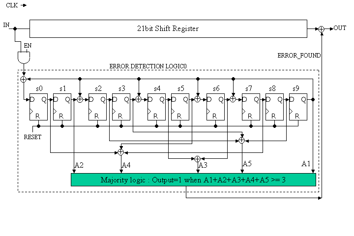
Figure 4: one example of the Receiver (LEVEL1)
Figure 5 shows the total system organization to be designed in this task. It consists of Transmitter, Receiver and Error-counter. You have to design the Receiver and the Error-counter. However, you need to synthesize the circuit of only Receiver. The Error-counter is only used for your evaluation.
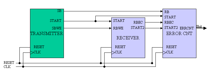
Figure 5: System Block Diagarm
(More explanation in TRANSMITTER)
TRANSMITTER generates 11 information bits U(x) and generates 10 parity bits R(x). Then totally 21 bits transmission packet SB(x) is generated. In addition, TRANSMITTER adds 21 bit predetermined sequence for synchronizing purpose before the 21 bits transmission packet. Then the total packet size is 42 bits. The predetermined sequence is from MSB to LSB "001101011110111000000". TRANSMITTER sends out MSB first.
In addition, TRANSMITTER generates some bit errors on the 42 bit packet. The transmission packet is output on the SBWE node. SBWE stands for Sent Bits With Error. 42 clock cycles are needed to output the one packet. This 42 cycle includes 11 information bits, 10 parity bits and 21 synchronizing bits.
START signal is also output to indicate which clock cycle the first information bit is coming out.
SB is sent-out bits without errors to check the functionality of RECEIVER.
(More explanation in RECEIVER)
RECEIVER receives the signal from TRANSMITTER 's SBWE. Using 21 bits in the 42 bit packet, error correction is performed. Then error-corrected 11 information bits are output at the node RBEC (Received bits Error Corrected). The RECEIVER knows the start timing of the information bits by START signal. However, LEVEL3 task needs to generate START signal not to use START input signal. Be sure to remember the 21 bits synchronizing sequence also might include some errors.
(More explanation in ERROR CNT)
ERRORCNT is the circuit block to evaluate the RECEIVER error correction functionality. From TRANSMITTER, it receives START siganl and SB signal. Since SB signal has no error, ERRORCNT always know the correct data transfer. Also, ERRORCNT receives the error-corrected signal by RECEIVER thru RBEC node. Then ERRORCNT compares RBEC with SB and counts how many miss error correction has happened. The accumulated error count is output at the node ERRCNT with 8 bit bus width, which means maximum 255 errors are countable.
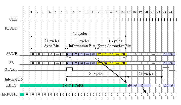
Figure 6: System Timing Diagram
Figure 6 shows the operational timing diagram. After the RESET desertion, TRANSMITTER outputs 42 bits packet and repeatedly sends out the packets every 42 cycles. The first 21 bits are Sync bits, then 11 information bits, then 10 error correction (parity) bits are sent out. The Sync Bits is "001101011110111000000". The RECEIVER receives SBWE signal and perform the error correction. The error corrected information is coming out at the node RBEC. The parity bits also can be error-corrected. But this is optional and depends on the applicants. ERRCNT shows the accumulated error counts and it has 8 bit width. But you can freely change the bit width.
The Internal EN signal is '1' during 21 cycles from the START assertion and '0' for other 21 cycles. This Internal EN signal is corresponding to the signal EN in figures 4 and 7. EN='1' means the period to get input data to syndrome registers and EN='0' means the period of ERROR_FOUND signal generation.
The beginners' task has the following pin lists.
|
Receiver |
|||
| signal name | in or out | bit width | explanation |
| CLK | IN | 1 | clock input |
| RESET | IN | 1 | assertion '1' means reset |
| START | IN | 1 | indication of the first information bit |
| RBWE | IN | 1 | received signal with error |
| START2 | OUT | 1 | indication of first information bit for RBEC |
| RBEC | OUT | 1 | error corrected result output |
Table 10: LEVEL1 pin list
Following are VHDL description of TRANSMITTER, TRANSMITTER, total test bench and RECEIVER template.
TRANSMITTER: transmitter.vhd
TRANSMITTER: errorcnt.vhd
Test bench: test_dcc21.vhd
RECEIVER template: receiver.vhd
LEVEL2 task has the same pin list as table10. But you have to use the following error correction circuit as shown in figure 7.
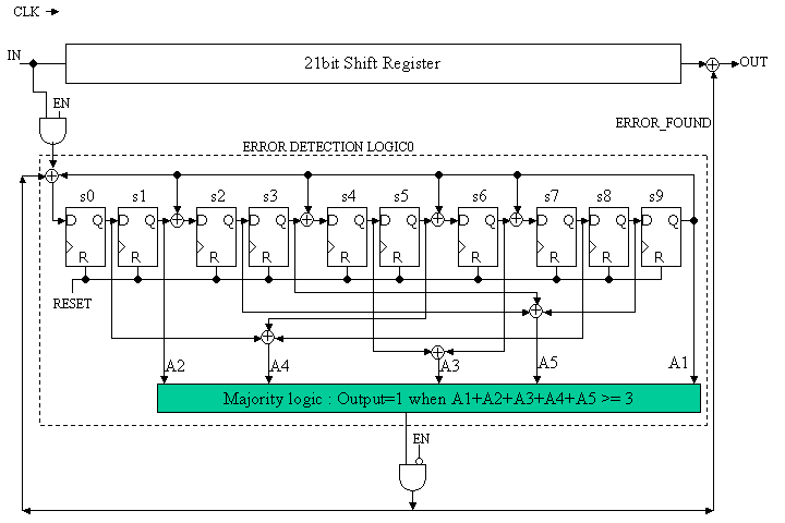
Figure 7: improved error detection logic
Figure 7 has additional feedback from ERROR_FOUND signal to syndrome registers. When error is found, the error will be corrected. Then this correction is fed back to the syndrome re-computation. Then once all error are corrected all syndrome register bits s0, s1, ..., s9 will be zeros. By this improvements, total error correction performance will be improved.
LEVEL3 TASK doen not use START signal and does use the LEVEL2's improved error detection logic. Since START input is not available, internal START signal has be generated using the 21 sync bits. Be sure to remember error happens even in the sync bits.
|
Receiver |
|||
| signal name | in or out | bit width | explanation |
| CLK | IN | 1 | clock input |
| RESET | IN | 1 | assertion '1' means reset |
| RBWE | IN | 1 | received signal with error |
| START2 | OUT | 1 | indication of first information bit for RBEC |
| RBEC | OUT | 1 | error corrected result output |
Table 11: LEVEL3 pin list
Since it is impossible to use the same synthesis library for various participants, use the 1 exor gate delay as a unit for speed comparison.
In the previous example, total delay = 7.17 ns and 6 circuit stages, then the 7.17/6= 1.195 ns is the unit of the speed. Please normalize your circuit speed by this unit.
| Title page | 1 | Team name, Members Name, School, Grade |
| 2 | Address, Phone, Email-address | |
| 3 | T-shirt size for all members in the team | |
| 4 | Which level of task is designed. | |
| Contents | 1 | Circuit block or architecture description |
| 2 | Designed circuit functional explanation, etc. | |
| 3 | Appealing point and originality | |
| 4 | Critical path speed, and circuit area | |
| 5 | HDL codes (VHDL or Verilog HDL) | |
| 6 | Simulation waveform indicating the design is operating! | |
| 7 | Anything you want to claim |
Report has to be emailed to the following address. Please use PDF file format.
If you want to send the report data other than PDF, please consult me.
ENJOY HDL! We want to see you at OKINAWA!