Tom Wada, Prof of the University of the Ryukyus, Information Engineering Dept.
This year's design target is the All Digital FM Receiver circuit. The FM (Frequency Modulation) is one of very famous wireless communication method and you can find many text book relating to the FM. Carrier frequency is modulated according to the strength of analog signal such as Voice. In this design project, we are going to design the all digital FM receiver circuit assuming the Frequency Modulated signal is converted to series of numerical values (digital signal) via Analog to Digital Conversion (ADC) circuit.
Since this contest is mainly for University students, we try to realize the target design as simple as possible. The core of the target design will be digital phase locked loop circuit, which generates sinusoidal wave synchronizing to the input FM wave. The requirements of the design is to write HDL (VHDL or Verilog HDL) and to synthesize digital circuits using Synopsys design analyzer or any other EDA tools. Making FPGA is also optional but our judges love to see your FPGA designs.

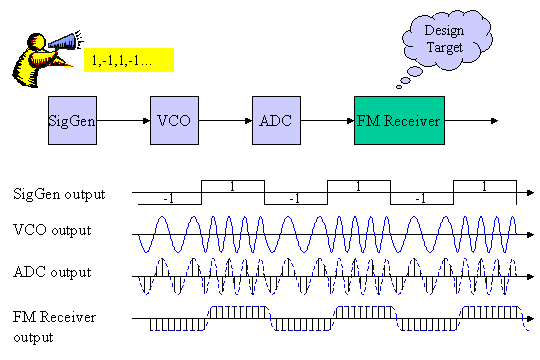
Figure1 System Diagram
Figure 1 shows the Frequency modulation and demodulation system. Signal generator (SigGen) generates the transmitting signal. In the figure 1, although only 1 or -1 are assumed for SigGen output, other value such as 0.5 is also acceptable. VCO represents Voltage Controlled Oscillator, which generates sinusoidal wave frequency-modulated by the SigGen output. ADC is Analog to Digital Converter, which converts the analog FM signal to descrete digitaized signals. When the output of SigGen is -1, the VCO output frequency is relatively low, and when the SigGen output is 1, the VCO output frequency is relatively high. In our design target, we assume the ADC output bit width is 8 bit. Then 28=256 different values can be expressed at the output of ADC. The FM Receiver gets the 8 bit signal every clock cycle and outputs the demodulated output.
The figure 2 shows the serially connnected PLL cirucit and Low Pass Filter circuit. This simple circuit configuration realizes the our target FM Receiver circuit.
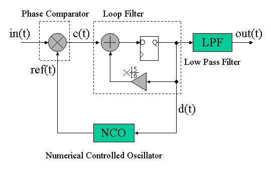
Figure 2. PLL and LPF
In this section, PLL operation basic will be explained using some mathematical equations.
Since the input signal is Frequency Modulated, the input signal in(t) can be expressed as follows,
![]()
NCO is similar oscillator as VCO. although VCO is analog circuit, NCO is digital circuit. The output sinusoidal frequency is controlled by digital input value. The the oscillator is called as Numerical Controlled Oscillator (NCO). As shown in figure 1, since the PLL includes the feedback loop, NCO outputs the same frequency sinusoidal with in(t). Then NCO output ref(t) is expressed as follows,
![]()
By multiplying in(t) and ref(t) gives the c(t) as follows,

The first term of the above equation corresponds to the phase difference between in(t) and ref(t). The second term corresponds to high frequency component. By removing the second term thru loop filtering, the phase difference can be obtained. This is the job of the Phase Comparator.
As shown in the figure 2, the loop filter circuit is composed of small loop circuit. It does addition of c(t) and coefficient alpha=15/16=0.9375 multiplied D flipflop output. Then loop filter output expressed as follows.
![]()
This is a kind of averaging with the smaller weight for the older values. Then it has low pass filtering characteristics.
NCO will be explained in the next section.
Figure 3 explains NCO.
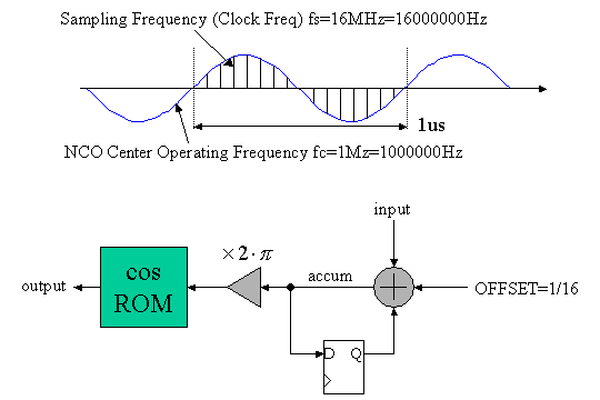
Figure 3. Numerical Controlled Oscillator (NCO)
In our target system, let's assume that system clock frequency is 16MHz = 16,000,000MHz and center NCO operating frequency is 1MHz = 1,000,000MHz. Then as shown in the figure 3, there are 16 sampling points in 1 cycle of 1MHz sinusoidal wave.
The NCO generates exactly 1 cycle of sinusoidal wave when input value = 0. Then the offset value is 1/16. Every clock cycle, the D flipflop accumulates the offset value. Then, in 16 cycles, accumulated value will increase by 1.0. The accumulator output is multiplied by 2pai, then cosine value is extracted from the cos ROM.
When the input value is more than 0, the accumulation speed gets higher. Then in less than 16 cycles, the accumulator increases by 1.0. This corresponds to higher frequency than 1.0MHz is generated. Vice versa, when the input value is less than 0, lower frequency than 1.0MHz is generated. Consequently, the NCO operating frequency will be controlled by the input value with center frequency of 1.0MHz.
One of the most famous digital filter is Finite Impulse Response (FIR) Filters. Figure 4(a) shows the 16 TAP FIR filter circuit diagram.
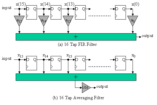
Figure 4. Finite Impulse Response Filters
Then, the 16TAP filter output is as follows,
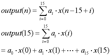
If the coefficients a0, a1, ..., a15 are appropriately determined, optimized Low Pass Filter can be configured. However, the optimized configuration needs 16 multipliers, that is, larger circuit area. Then, in this design task, let's assume the all coefficients ai = 1/16=0.0625. Figure 4(b) shows this configuration. 1/16 multiplier is moved to the latter stage and shared. In reality, 1/16 multiply can be implemented by just 4 bit right shift operation. Then, no multiplier is required.
In this design task, we need to treat fraction number such as 1/16 = 0.0625 in digital circuit design. The meaning of the 4 bit value "0111" does change according to the position of the fraction point. For example, "01.11" in binary means +1.75 in decimal, and "0111." in binary means +7 in decimal. In addition, the meaning of the 4 bit binary value will change whether it is unsigned format or two's complement format. For example, "11.10" in unsigned binary means + 3.50 in decimal, and "11.10" in two's complement binary means -0.50 in decimal.
Then we need to clarify the attributes of both "the position of fraction point" and "unsigned or two's complement" when we use binary number.
In this section, the attributes notation , which is used in Signal Processing Workbench, is explained.
If the signal attribute is <8,2,t>, then the signal is as follows,
8: signal width is 8 bit
2: integer part is 2 bits
t: two's complement number, then the MSB bit of the signal is sign bit.
For example, "01101111" with attribute <8,2,t> is as follows.
| 0 | 1 | 1 | 0 | 1 | 1 | 1 | 1 |
| sign bit | integer |
fraction |
|||||
Then fraction is 5 bits and it is +3.46875 in decimal.
If the signal attribute is <8,2,u>, then the signal is as follows,
8: signal width is 8 bit
2: integer part is 2 bits
u: unsigned format, then the value is always positive or zero and no sign bit.
For example, the same "01101111" with attribute <8,2,u> is as follows.
| 0 | 1 | 1 | 0 | 1 | 1 | 1 | 1 |
| integer | fraction | ||||||
Then the fraction is 6 bits and it is +1.734375 in decimal.
The more integer bits corresponds to the wider range. The more fraction bits corresponds to the higher resolution.
Table 1 shows the comparison between <4,2,u> and <4,1,t>.
Table 1. comparison by the attribute
4bit binary decimal value in case of <4,2,u> decimal value in case of <4,1,t> 0000 +0.00 +0.00 0001 +0.25 +0.25 0010 +0.50 +0.50 0011 +0.75 +0.75 0100 +1.00 +1.00 0101 +1.25 +1.25 0110 +1.50 +1.50 0111 +1.75 +1.75 1000 +2.00 -2.00 1001 +2.25 -1.75 1010 +2.50 -1.50 1011 +2.75 -1.25 1100 +3.00 -1.00 1101 +3.25 -0.75 1110 +3.50 -0.50 1111 +3.75 -0.25
Table 2 shows some attributes examples. Same 4 bit width binary can be used to express various ranges and resolutions.
Table 2. Attributes examples (binary representation, range, resolution)
attributes binary representation
S: sign bit
X: data bitrange resolution integer <1,1,u> X. 0 to 1 1 <4,4,u> XXXX. 0 to 15 1 <4,3,t> SXXX. -8 to 7 1 fraction <4,0,u> .XXXX 0.0 to 0.9375 0.0625 (1/16) <4,0,t> S.XXX -1.00 to +0.875 0.125 (1/8) others <4,2,u> XX.XX 0.0 to 3.75 0.25 (1/4) <4,2,t> SXX.X -4.0 to + 3.5 0.5 (1/2) <4,5,u> XXXX0. 0 to 30 2 <4,5,t> SXXX00. -32 to 28 4 <4,-1,u> .0XXXX 0.0 to 0.46875 0.03125 (1/32) <4,-1,t> S.SXXX -0.5 to +0.4375 0.0625 (1/16)
Figure 5 shows a example circuit diagram of the FM receiver with all bit attributes. fmin is 8bit FM input signal and dmout is 12 bits demodulated output signal.
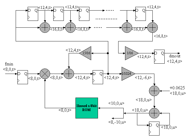
Figure 5. A example of All Digital FM Receiver
Figure 6 shows the simulated waveform of the example circuit. Here, the system clock frequency and the sampling frequency are 16MHz = 16,000,000Hz. FM modulation is +- 10KHz at center of 1MHz=1,000,000Hz. The modulation is just +-10% of the 1MHz carrier frequency, then it is difficult to identify the FM modulation in the figure 5 simulation waveform. In the simulation, we have assumed the sampling frequency = 16MHz. However, you can scale the sampling frequency as you wish. Be sure not to forget to scale the carrier frequency.
The first row shows the sending data is repeating 1 and -1. The second row show the FM modulated waveform according to the sending data. The third row is NCO output and the fourth row is Phase comparator, that is, multiplier output. The fifth row and the sixth row are the accumulator output and the demodulated output. In this view, all sampled signal, which are discrete, are connected in line. At the initial simulation phase, the demodulated output overshoots since the phase synchronization is in convergence phase.
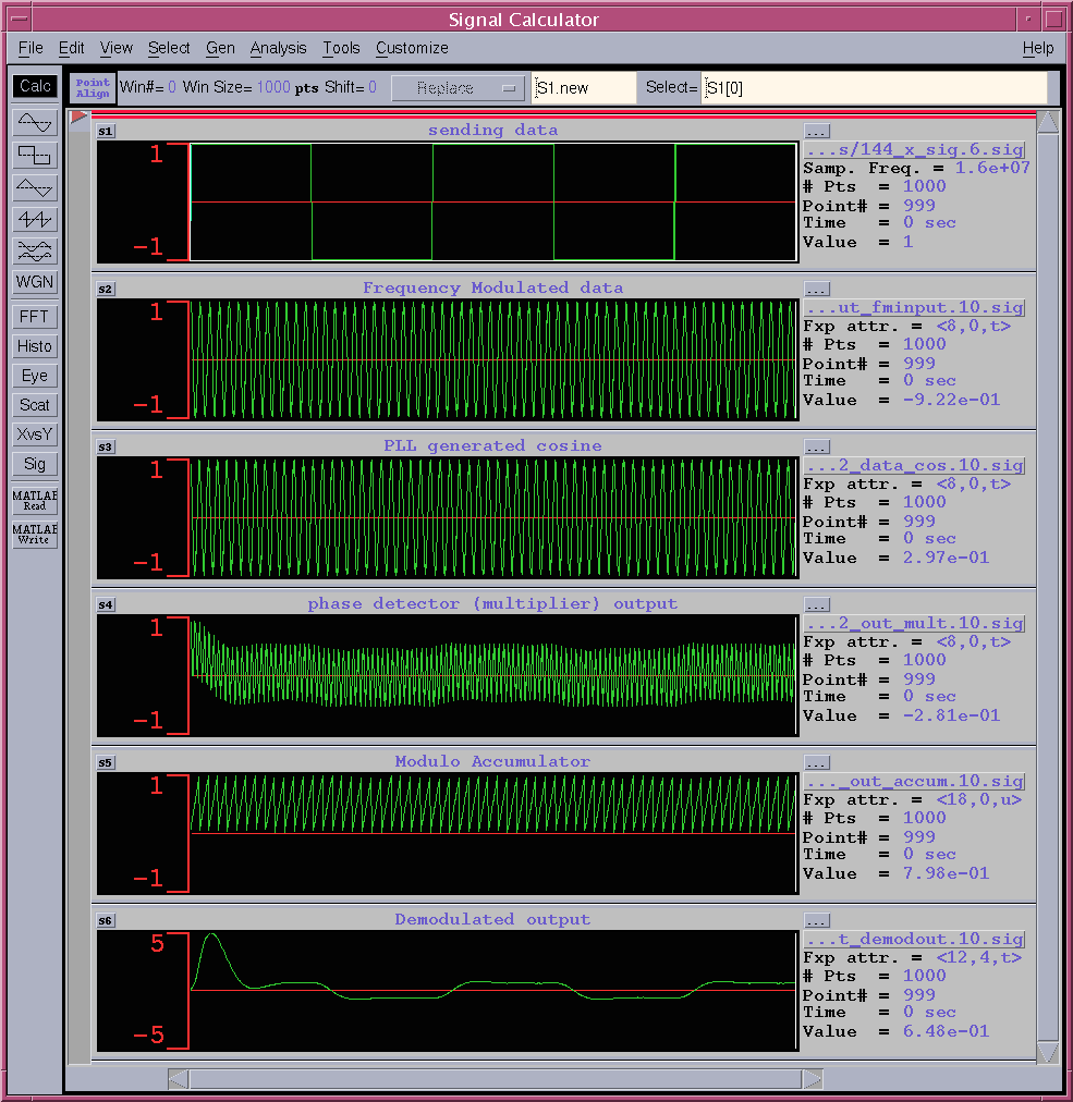
Figure 6. Simulated Waveform (1)
A part of the figure 6 is expanded and shown in figure 7. In this view, all sampled signal is shown in bar graph style.
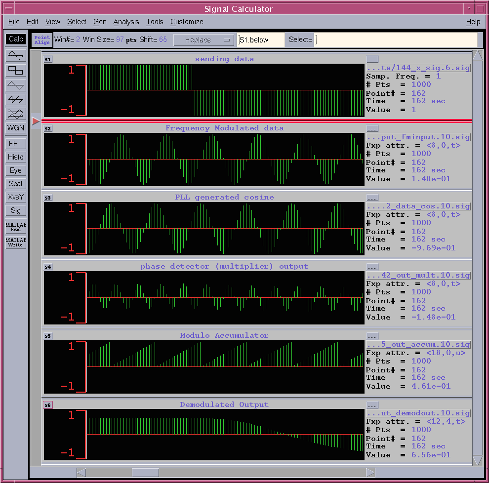
Figure 7. Simulated Waveform (2)
In LEVEL 1 Task, the minimum design requirement is to design FM demodulation circuit which is capable to demodulate the 1 and -1 repeating sending data as shown in figure 6. Table 3 shows the example of the pin list of the FM Receiver. You can modify the pin list if needed.
Table 3. Pin list for LEVEL1
|
FM Receiver |
|||
| Signal name | in or output | bit width | explanation |
| CLK | IN | 1 | system clock input |
| RESET | IN | 1 | assertion '1' means reset |
| FMIN | IN | 1 | input data with attribute<8,0,t> |
| DMOUT | IN | 12 | demodulated output with attribute<12,4,t> |
FM input (FMIN) data is linked as follows, corresponding to the second row waveform in figure 6. The attribute is <8,0,t> and 1000 points.
FM input: fm.txt
NCO's cos ROM data is also linkd as follows. It just one cycle of cosine then it it will be easily generated. Totally 1024 <8,0,t> data.
x=0 to 1023 by 1, cosine value = cos(2*pi*x/1024)
cosine ROM contents: cos.txt
In LEVEL 2 Task, the minimum design requirement is to design FM demodulation circuit which is capable to demodulate the triangular wave between -1 to 1 as shown in figure 8. According to the sixth row of figure 8, you can see that the triangular sending data is successfully demodulated. Input data vector is linked as follows.
FM input wave for triangular sending data with attribute <8,0,t>: fmTri.txt
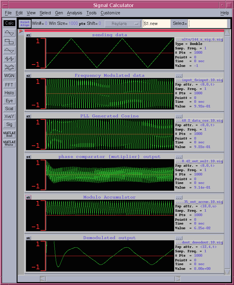
Figure 8. Simulated waveform for Triangular shape sending data
Since it is impossible to use the same synthesis library for various participants,
In the previous example, total delay = 7.17 ns and 6 circuit stages, then the 7.17/6= 1.195 ns is the UNIT_DELAY of the speed. Please normalize your circuit speed by this UNIT_DELAY.
In the example, total cell area = 147.0 and 49 EXOR gates. Then 147.0/49=3.0 is the UNIT_AREA. Please normalize your circuit area by this UNIT_AREA.
| Title page | 1 | Team name, Members Name, School, Grade |
| 2 | Address, Phone, Email-address | |
| 3 | T-shirt size for all members in the team | |
| 4 | Which level of task is designed. | |
| Contents | 1 | Circuit block or architecture description |
| 2 | Designed circuit functional explanation, etc. | |
| 3 | Appealing point and originality | |
| 4 | Critical path speed, and circuit area | |
| 5 | HDL codes (VHDL or Verilog HDL) | |
| 6 | Simulation waveform indicating the design is operating! | |
| 7 | Anything you want to claim |
Report has to be emailed to the following address. Please use PDF file format.
If you want to send the report data other than PDF, please consult me.
Thank you Mr. Akihisa Yokoyama @ TOYOTA INFO-TECHNOLOGY CENTER for providing initial circuit idea of FM receiver.
This program is
operated by Univ. of Ryukyus, IE dept.,
co-operated by Okinawa Industry Support Center,
and co-sponsored by SONY LSI Design Inc and
Kyusyu Bureau of Economy, Trade and Industry.
ENJOY HDL! We want to see you at OKINAWA!