2006/9/19
Tom Wada, Prof of the University of the Ryukyus, Information Engineering Dept.
This years LSI Design Contest in OKINAWA 2006 is the 10th ANNIVERSARY contest. Originally, the LSI contest has been started from the design contest inside the Department of Information Engineering in University of the Ryukyus at 1998. From 2000, the contest has been opened to outside students and from 2001 the contest is co-operated with CQ publishing corporation and is opened to international students. In resent years, roughly one hundred students are trying to solved the LSI design contest task. In the Table 1, all design themes are shown.
| year | Design Theme | Application | |
| 1 | 1998 | KUE-CHIP | Micro-processor |
| 2 | 1999 | RSA encription decoder | cipher |
| 3 | 2000 | Galois Matrix Multiplier | Forward Error Correction |
| 4 | 2001 | Digital CDMA Receiver | Cellar phone, WLAN |
| 5 | 2002 | Error Correction Circuit Using Difference-set Cyclic code | Character Broadcast Service, Terrestrial Video Broadcast |
| 6 | 2003 | Variable-Length Decoder for Static Huffman Code | Sound compresion, Image compression |
| 7 | 2004 | SubBytes Transform circuit for AES Cipher | WLAN, code, cipher |
| 8 | 2005 | All Digital FM receiver | Wireless communication, Broadcasting |
| 9 | 2006 | 2-D Product code Iterative Decoder | Wide Area LAN |
| 10 | 2007 | 64 point Fast Fourier Transform Circuit | Signal Analysis, OFDM, WLAN |
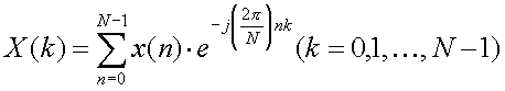
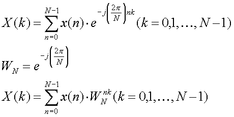
The 10th anniversary year design theme is Fast Fourier Transform Circuit, which is very famous signal processing technology. the FFT is the algorithm to reduce computation of Discrete Fourier Transform (DFT). This contest task is 64 point FFT, which is used in 802.11a/g/n Wireless LAN devices. The equation of FFT is shown as follows. This time N is 64.
Although the equation is simple, the input signal x(n) is 64 point complex values and the output X(k) is 64 points complex values. Then the actual computation is not small. In the following section, the detail description of FFT will be shown step by step. Then please try this contest task even you are not familiar with the FFT. The requirements of the design is to write HDL (VHDL or Verilog HDL) and to synthesize digital circuits using Synopsys design analyzer or any other EDA tools. Making FPGA is also optional but our judges love to see your FPGA designs.
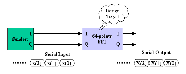
Figure 1 System Diagram
Figure 1 show the block diagram of the system. The system is composed of two parts, Signal Sender and FFT. Since the inputs and outputs signals are series of complex values, I port is used for Real component of the complex and Q port is for Imaginary component of the complex value. All 64points are input to FFT serially as shown in the figure. The FFT output is also serial manner. The head position of the series is indicated by another HEAD signal, although it is now shown in the figure.
One famous application of DFT is spectrum analysis of a signal. One typical application is shown in figure 2. x(n) signal is analyzed signal and total N points. The x(n) signal is roughly one cycle signal in duration N points. DFT of x(n) results X(k). At k=1, |X(k)| has a large peak. This means x(n) has a element of one cycle per N points frequency components. In addition, at k=N-1, another peak is observed. The N points DFT output has cyclic characteristics. Then index k=N-1 has the meaning of k=-1, that is, Negative frequency. Since the signal x(n) signal (Real Signal) is composed of k=1 positive and k=-1 negative frequency components, X(k) has k=1 and -1 components.
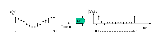
Figure 2 Spectrum analysus by Discrete Fourier Transform
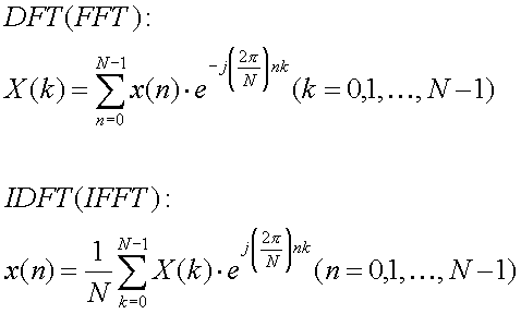
Following are equations of Discrete Fourier Transform (DFT) and Inverse Discrete Fourier Transform (UDFT). N points x(n) signal is transformed to N points X(k) by DFT. Fast computation algorithm of DFT is Fast Fourier Transform (FFT). But, FFT needs the restriction N=2l (l=integer). IFFT is Fast computation algorithm of IDFT.
If we take a look at those FFT and IFFT equation. Looks like very similar but two differences.
1) Divided by N
2) sign of power of exponential
Since the differences are small, if we have FFT circuit then IFFT can be made as Figure 3.
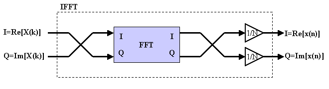
Figure 3 IFFT circuit made by FFT module
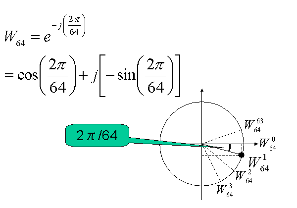
Since the design task is FFT, let's take a look at FFT algorithm more deeply. Here we introduce a Twiddle Factoe WN. The FFT equation can be rewriitten as follows.
Twiddle means "Turn around with fingers" then it is the factor of rotation.
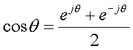
Please have imagination of 2 dimensional surface with two axis Real and Imaginary (complex surface). According to the Euler's law ejθ is as follows. If we change θ, ejθgoes round on radious=1 circle on the complex surface. Then this ejθindicates the rotation.
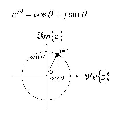
Figure 4 Euler's law and complex surface
In another word, this rotation function ejθis called complex sinusoid. In the Fourier Transform, the signal is analyzed using this complex sinusoid. Counter-clockwise rotation corresponds to positive frequency and clockwise rotation corresponds to negative frequency.
Then the twiddle factor WN indicated on the complex surface is shown in Figure 5. (WN)m is simply m-times rotation of WN. When m is increased, the point is rotating on the circle.
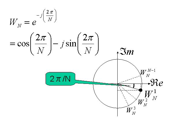
図5 Twiddle Factorの意味
In order to understand the FFT more visually, 4 point FFT equation is converted to matrix notation in figure 6. In the matrix notation, 4X4 twiddle factor matrix appears. The 1st row has all 4 W0. In the second row, twiddle factor is rotating on the circle once with clockwise direction. In the third row, twiddle factor is rotating on the circle twice. In the 4th row, twiddle factor is rotation on the circle onece with counter-clockwise direction and this can be considered as three-times rotation with clockwise direction.
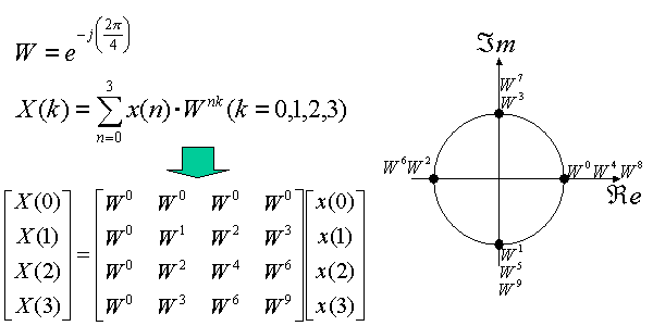
Figure 6 Matrix representation of 4 points FFT
Figure 7 shows this rotation visually.
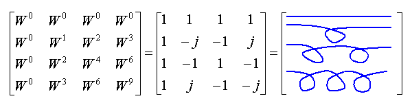
Figure 7 Twiddle factor matrix of 4 points FFT
Usually in digital signal processing text books, FFT computation uses Butterfly circuit, especially it is radix-2 butterfly. However, in this section, FFT computation with radix-4 butterfly will be explained since the radix-4 butterfly needs less computation recourses.
Because of 64=43, FFT index is changed as follows. There are 3 Σ computations. This corresponds to Three stages architecture.
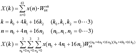
First expand the summation relationg to n2. Here, Characteristics of twiddle Factor WN, 、(WN)0=1, (WN)1N/4=-j, ( WN)2N/4=-1, ( WN)3N/4=j are used.
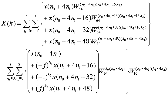
Here we introduce the x1 as follows, then
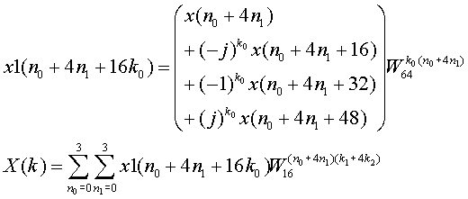
This x1 computation is the TASK at the first stage. Then the following stages gets the result of the 1st stage as input and compute X(k). Actually this is same as 16 point FFT. However, there are 4 cases k0=0, 1, 2, 3 . As a result 4 times 16 points FFT computation is needed in the following stages.
Each x1 computation needs 4 inputs then we call this comtation as radix-4 butterfly.
Next expand the summation relationg to n1. And here we introduce the x2 as follows, then
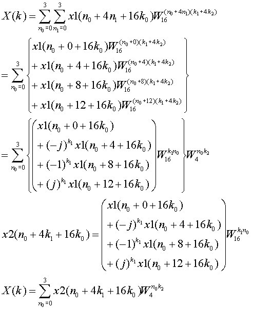
Consequently the STAGE 2 computes x2. This is also same as radix 4 computation.
Again the summation relationg to n0.
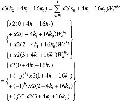
In this 3rd stages, no twiddle factor computation is needed.
At the stage 3, x3(k2+4K1+16K0) is computed. However, original index was (k0+4K1+16K2). Then the index values are exchanged. Then in order to have correct index, x3 results have to be re-ordered based on the following equation.
![]()
As a conclusion, 64 points FFT computation based on radix-4 method needs totally 4 stages including re-order. The computation architecture is shown in figure 8.
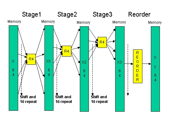
Figure 8 RADIX-4 64 points FFT architecture
Here we provide radix-4 64 points FFT by MATLAB code: myfft64.m
Since in order to fully understands the FFT computation, to read MATLAB code is one good method. Please pay attention that in MATLAB index starts from 1 not 0.
In addition, we also provide radix-4 64 points FFT by SCLLAB code : myfft64.sce
SCILAB is similar SCIENTIFIC calculation software which is available in the following URL as a Free S/W.
Here we also provide our simple memo on SCILAB: HowToScilab.pdf
Here we introduce one circuit implementation example, which is shift-register-based serial processing FFT.
According the section 3, Stage 1 needs 16-point apart 4 inputs and computes 16-point apart 4 outputs. In stage 2, 4-point apart 4 inputs are needed, and in stage 3, neighboring 4 inputs are needed.
(Stage 3 serial computation)
The Stage 3 computation can be processed as follows (Figure 9). The rectangle block means shift registers. Input data are serially coming into the shift registers. There are total 7 shift registers. Every clock, the input are shifting. By controlling the multiplexer, 4 inputs which is needed for radix-4 butterfly are inputted to the butterfly circuit.
The butterfly circuit has to multiply 1, j, -1, -j to the inputs. However, this multiply is just exchange I (Real) and Q (Imaginary) components and change sign. Then actual implementation can be done with multiplexer and adders. The output of the butterfly has to be multiplied with twiddle factor. Then complex multiplier is needed. But, in stage 3 only, twiddle factor is always 1.
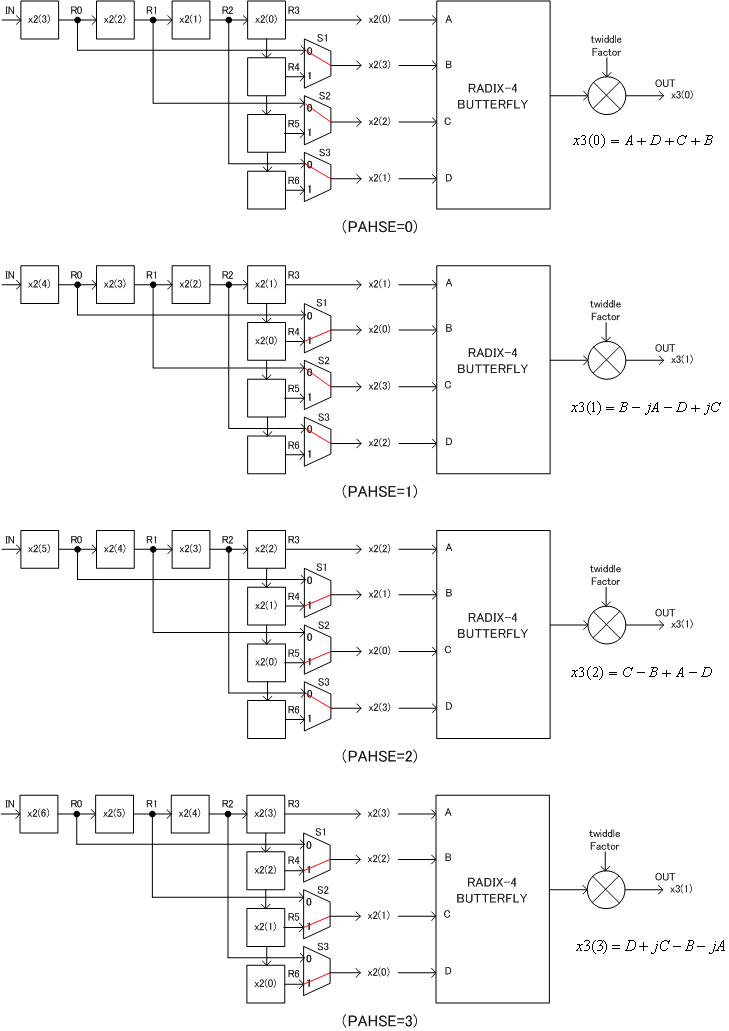
Figure 9 Stage 3 serial processing architecture
Figure 10 shows the operation waveform of the Stage 3. HEAD signal is asserted at the beginning of the signal. The 4 yellow points are first radix-4 inputs. R0 to R6 shows the signal of the shift registers. PHASE signal has to be generated from HEAD signal assertion. S1, S2, S3 swicth signals, which controlle the multiplexers, are generated from the PHASE signal.
A, B, C, D signals are inputs to the butterfly circuit and during 4 cycles same 4 signals appearing by some rotation. During this 4 cycles 4 radix-4 butterfly computation is executed to generate OUT signal. OUT_HEAD signal indicates the beginning of the output sequences.
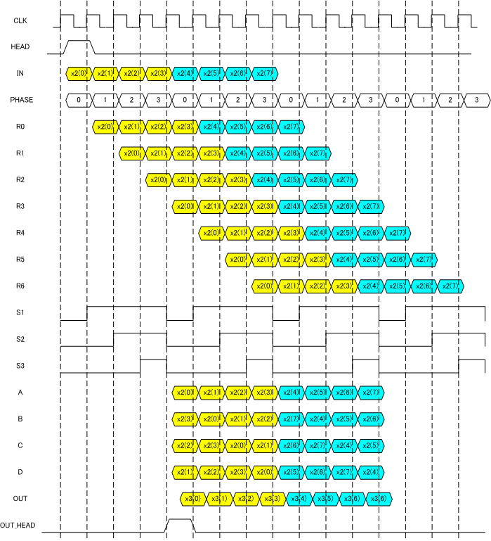
Figure 10 Stage 3 operating waveform
Other stage procesing can be realized by changing the shift register length of stage 3 circuit. Of couese, twiddle factor generation and complex multiply is needed. Figure 11 shows the case of stage 2 as a example.
Since 4-point apart input signals are needed to butterfly computation in stage 2, there are 4 stages between each of R0, R1, R2, R3, R4, R5, R6 registers. In this case continuous 4 points processing needs same PHASE state. Then, every 4 cycles PHASE counts up. For Stage 1 there needs 16 shift registers between each of R0, R1, R2, R3, R4, R5, R6 registers.
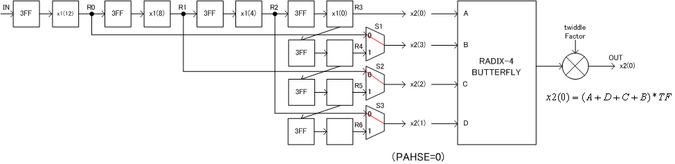
Figure 11 Stage 2 example
As explained in the previous section, following reorder has to be implemented.
![]()
This means x3(0), x3(1), x3(2), x3(4), ... outputs corresponds to X(0), X(16), X(32), ...outputs. In Table 2 detail reordering relation is shown. If you take a look at the table well, there are some rules. The reorder can be implemented using shift registers and/or memories.
| x3(k2+4k1+16k0) | X(k0+4k1+16k2) | x3(k2+4k1+16k0) | X(k0+4k1+16k2) | x3(k2+4k1+16k0) | X(k0+4k1+16k2) | x3(k2+4k1+16k0) | X(k0+4k1+16k2) | |||
| 0 | 0 | 16 | 1 | 32 | 2 | 48 | 3 | |||
| 1 | 16 | 17 | 17 | 33 | 18 | 49 | 19 | |||
| 2 | 32 | 18 | 33 | 34 | 34 | 50 | 35 | |||
| 3 | 48 | 19 | 49 | 35 | 50 | 51 | 51 | |||
| 4 | 4 | 20 | 5 | 36 | 6 | 52 | 7 | |||
| 5 | 20 | 21 | 21 | 37 | 22 | 53 | 23 | |||
| 6 | 36 | 22 | 37 | 38 | 38 | 54 | 39 | |||
| 7 | 52 | 23 | 53 | 39 | 54 | 55 | 55 | |||
| 8 | 8 | 24 | 9 | 40 | 10 | 56 | 11 | |||
| 9 | 24 | 25 | 25 | 41 | 26 | 57 | 27 | |||
| 10 | 40 | 26 | 41 | 42 | 42 | 58 | 43 | |||
| 11 | 56 | 27 | 57 | 43 | 58 | 59 | 59 | |||
| 12 | 12 | 28 | 13 | 44 | 14 | 60 | 15 | |||
| 13 | 28 | 29 | 29 | 45 | 30 | 61 | 31 | |||
| 14 | 44 | 30 | 45 | 46 | 46 | 62 | 47 | |||
| 15 | 60 | 31 | 61 | 47 | 62 | 63 | 63 |
In this design task, we need to treat fraction number such as 1/16 = 0.0625 in digital circuit design. The meaning of the 4 bit value "0111" does change according to the position of the fraction point. For example, "01.11" in binary means +1.75 in decimal, and "0111." in binary means +7 in decimal. In addition, the meaning of the 4 bit binary value will change whether it is unsigned format or two's complement format. For example, "11.10" in unsigned binary means + 3.50 in decimal, and "11.10" in two's complement binary means -0.50 in decimal.
Then we need to clarify the attributes of both "the position of fraction point" and "unsigned or two's complement" when we use binary number.
In this section, the attributes notation , which is used in Signal Processing Workbench, is explained.
If the signal attribute is <8,2,t>, then the signal is as follows,
8: signal width is 8 bit
2: integer part is 2 bits
t: two's complement number, then the MSB bit of the signal is sign bit.
For example, "01101111" with attribute <8,2,t> is as follows.
| 0 | 1 | 1 | 0 | 1 | 1 | 1 | 1 |
| sign bit | integer |
fraction |
|||||
Then fraction is 5 bits and it is +3.46875 in decimal.
If the signal attribute is <8,2,u>, then the signal is as follows,
8: signal width is 8 bit
2: integer part is 2 bits
u: unsigned format, then the value is always positive or zero and no sign bit.
For example, the same "01101111" with attribute <8,2,u> is as follows.
| 0 | 1 | 1 | 0 | 1 | 1 | 1 | 1 |
| integer | fraction | ||||||
Then the fraction is 6 bits and it is +1.734375 in decimal.
The more integer bits corresponds to the wider range. The more fraction bits corresponds to the higher resolution.
Table 3 shows the comparison between <4,2,u> and <4,1,t>.
Table 3. comparison by the attribute
4bit binary decimal value in case of <4,2,u> decimal value in case of <4,1,t> 0000 +0.00 +0.00 0001 +0.25 +0.25 0010 +0.50 +0.50 0011 +0.75 +0.75 0100 +1.00 +1.00 0101 +1.25 +1.25 0110 +1.50 +1.50 0111 +1.75 +1.75 1000 +2.00 -2.00 1001 +2.25 -1.75 1010 +2.50 -1.50 1011 +2.75 -1.25 1100 +3.00 -1.00 1101 +3.25 -0.75 1110 +3.50 -0.50 1111 +3.75 -0.25
Table 4 shows some attributes examples. Same 4 bit width binary can be used to express various ranges and resolutions.
Table 4. Attributes examples (binary representation, range, resolution)
attributes binary representation
S: sign bit
X: data bitrange resolution integer <1,1,u> X. 0 to 1 1 <4,4,u> XXXX. 0 to 15 1 <4,3,t> SXXX. -8 to 7 1 fraction <4,0,u> .XXXX 0.0 to 0.9375 0.0625 (1/16) <4,0,t> S.XXX -1.00 to +0.875 0.125 (1/8) others <4,2,u> XX.XX 0.0 to 3.75 0.25 (1/4) <4,2,t> SXX.X -4.0 to + 3.5 0.5 (1/2) <4,5,u> XXXX0. 0 to 30 2 <4,5,t> SXXX00. -32 to 28 4 <4,-1,u> .0XXXX 0.0 to 0.46875 0.03125 (1/32) <4,-1,t> S.SXXX -0.5 to +0.4375 0.0625 (1/16)
Suppose two real values a and b, complex value can be a + jb. Here,
![]()
Then two complex value a+jb and c+jd can be added as follows.
![]()
Then, complex addition just needs two real adders
(MULTIPLICATION)
two complex value a+jb and c+jd can be multiplied as follows.
![]()
Then, complex multiply needs 4 real multiplier and 1 subtraction and 1 addition.
Figure 12 shows examples of the circuits.
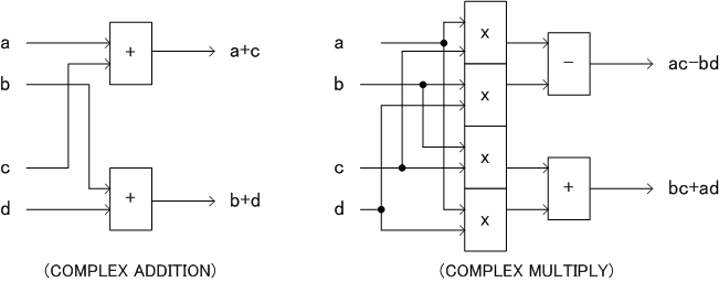
Figure 12 complex computation
64 points FFT design needs (W64)0 to (W64)63 64 complex values as shown in figure 13. The real (I) component is cosine and the imaginary components (Q) is -sin. Then the two 64 word ROM can be used to store twiddle factor.
Here we provide, two 64 word x 10 bit ROM data. The 10 bit format is <10,0,t>.
real = cos (2*π*address/64) : cos.txt
imag = -sin (2*π*address/64) : msin.txt
In this level, designner must assume input signal coming in serially with HEAD signal as shown in figure 14. Design FFT circuit which generate FFT outputs and OUTHEAD signal with some latency. The latency is arbitrary.
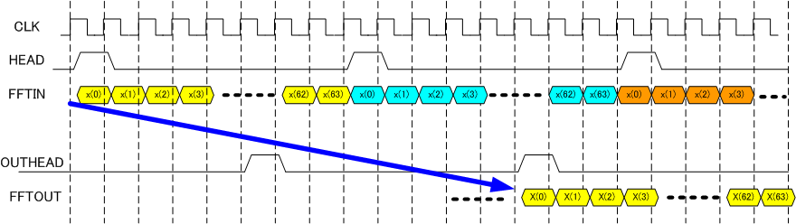
Figure 14 Task waveforms
Table 5 pin list
|
FFT |
|||
| Signal name | in or out | bit width | explanation |
| CLK | IN | 1 | Clock |
| HEAD | IN | 1 | '1' means the beginning |
| FFTIN_I | IN | 8 | Input Real components, <8,0,t>format |
| FFTIN_Q | IN | 8 | Input Imaginary components, <8,0,t>format |
| OUTHEAD | OUT | 1 | '1' means the beginning |
| FFTOUT_I | OUT | 14 | Output Real components, <14,6,t>format |
| FFTOUT_Q | OUT | 14 | Output Imaginary components, <14,6,t>format |
Following are 5 input and output signal examples.
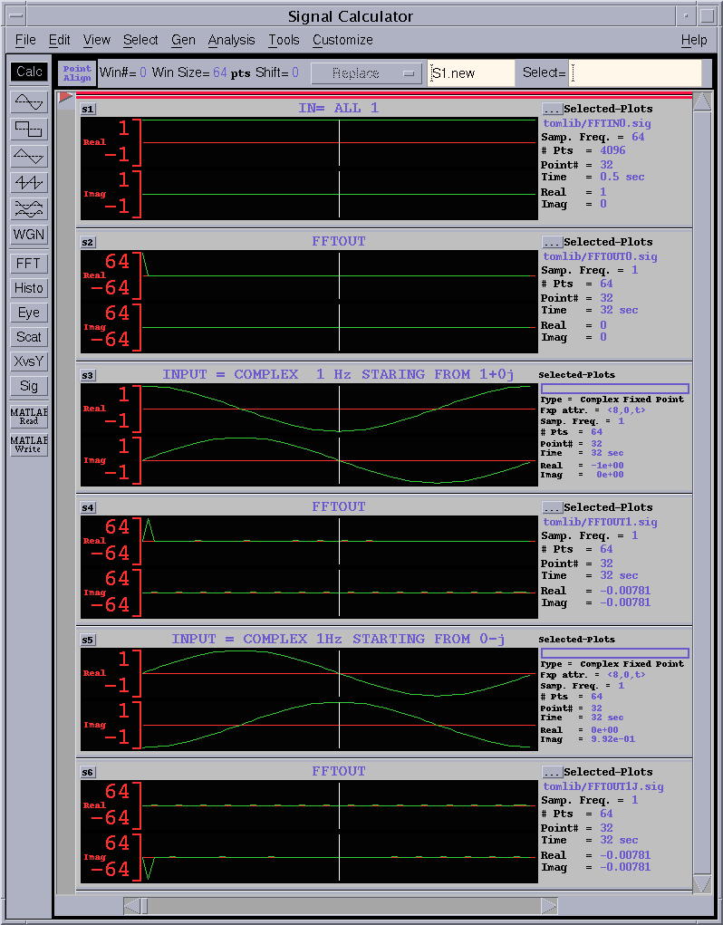
Figure 15 operation waveform (1)
The 1st wave of figure 15 is 1+0j fixed inputs. The corresponding outputs is the 2nd waveform. At index=0, 64.0 outputs and all 0 s for other index.
The 3rd waveform is one cycle complex sinusoid inputs. Input= cos(2*pi*n/64) + j sin(2*pi*n/64) n=0...63. The 4th FFT output has peak of 64.0 at index=1.
The 5th input is also one cycle complex sinusoid. However, the initial value is different. Input=sin(2*pi*n/64) - j cos(2*pi*n/64). Similarly with 3), the 6th FFT output has peak of -64.0j at index = 1.
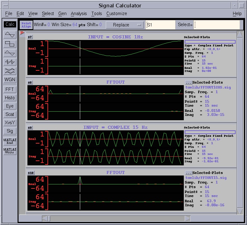
Figure 16 operation waveform (2)
The 1st waveform in figure 16 is cosine signal. Since cosine can be re-written as follows by Euler's law,
cosine signal has two different frequency of complex sinusoid of +1Hz and -1Hz with amplitude = 0.5. The the 2nd FFT output has two peaks of 32.0 (half of case 2, 3) at index = 1 and 63. According to FFT cyclic property, 63 can thought -1.
The 3rd waveform is 15 cycle complex sinusoid input. Then the 4th FFT output has peak of 64.0 at index = 15.
ALL 1 input: REAL FFTIN0REAL.txt , IMAGINARY FFTIN0IMAG.txt
One cycle complex sinusoid with initial value = 1 + 0j : REAL FFTIN1REAL.txt , IMAGINARY FFTIN1IMAG.txt
One cycle complex sinusoid with initial value = 0 - 1j: REAL FFTIN1JREAL.txt , IMAGINARY FFTIN1JIMAG.txt
One cycle cosine signal: REAL FFTIN1COSREAL.txt , IMAGINARY FFTIN1COSIMAG.txt
15 cycle complex sinusoid: REAL FFTIN15REAL.txt , IMAGINARY FFTIN15IMAG.txt
If you have a interesting, different, novel, surprising idea relating to this FFT design. You can modify the specification given in [8]. Please design unique circuit.
Since it is impossible to use the same synthesis library for various participants,
In the previous example, total delay = 7.17 ns and 6 circuit stages, then the 7.17/6= 1.195 ns is the UNIT_DELAY of the speed. Please normalize your circuit speed by this UNIT_DELAY.
In the example, total cell area = 147.0 and 49 EXOR gates. Then 147.0/49=3.0 is the UNIT_AREA. Please normalize your circuit area by this UNIT_AREA.
In order to make easy comparison among many design entries. Please follow the guide on ROM and/or RAM in your design.
| Title page | 1 | Team name, Members Name, School, Grade |
| 2 | Address, Phone, Email-address | |
| 3 | T-shirt size for all members in the team | |
| 4 | Which level of task is designed. | |
| Contents | 1 | Circuit block or architecture description |
| 2 | Designed circuit functional explanation, etc. | |
| 3 | Appealing point and originality | |
| 4 | Critical path speed, and circuit area, how many bit errors for each SNR | |
| 5 | HDL codes (VHDL or Verilog HDL) | |
| 6 | Simulation waveform indicating the design is operating! | |
| 7 | Anything you want to claim |
Report has to be emailed to the following address. Please use PDF file format.
If you want to send the report data other than PDF, please consult me.
This program is
operated by Univ. of Ryukyus, IE dept.,
co-operated by Okinawa Industry Support Center,
and co-sponsored by SONY LSI Design Inc and
Kyusyu Bureau of Economy, Trade and Industry.
ENJOY HDL! We want to see you at OKINAWA!