VLSI 2012 FINAL TASK の TASK1
2013/01/22
琉球大学工学部情報工学科 和田 知久
[0] LEVEL1 TASK
LEVEL 1 TASKでは、
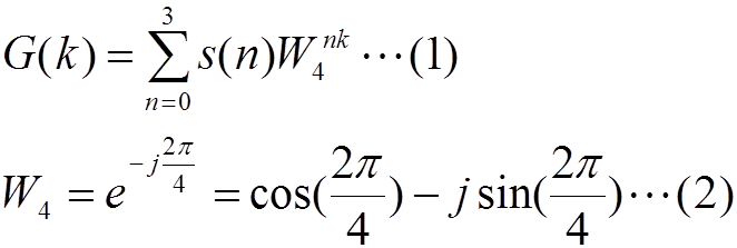
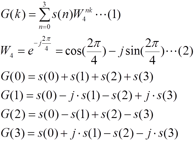
入力s(0), s(1), s(2), s(3)は4つの複素数入力であり、以下の式(1)、(2)にしたがって、G(0), G(1), G(2), G(3)なる複素数を計算する。
この動作をするアセンブラーコードをROM上に作成し、
プロセッサの機能として、32ビットどうしの乗算命令やシフト命令などを必要に応じて追加し、
RAM上に記憶した入力データに対して、プログラムを実行し、4点DFT結果をRAM上に出力する。
COSやSINの値が必要であれば、必要に応じて、値をRAM上に用意すること。
[1] 複素数フォーマット
LEVEL1TASKでも、前回やった同じ複素数のそーマットを使用することにととし、
複素数sr + j*si で、sr、siはそれぞれ16ビットとし、srとsiを連接して32ビットとして、主記憶に記憶する。
sr, siは各16ビットであるが、以下のように小数点の位置があると仮定する。最上位ビットMSBは符号を表し、2の補数表現とする。
|
固定小数点フォーマット |
例1 |
例2 |
|
SXXX XX . XX XXXX XXXX |
0000 00 .10 0000 0000 = 0.5(10進数) |
1111 11. 10 0000 0000 = -0.5(10進数) |
*** 小数点の位置を当初から変更している 注意! 注意! ***
[2] LEVEL0 TASK の実現実習
上記(1)式を計算するために、以下のような実装方法を考える。
(1)メモリ内の変数
データメモリ上に、S(0), S(1), S(2), S(3), G(0), G(1), G(2), G(3)およびW(0), W(1), W(2), W(3)を用意する。
S(n)は式(1)のDFT計算の入力複素数であり、G(k)はDFT計算の出力複素数である。
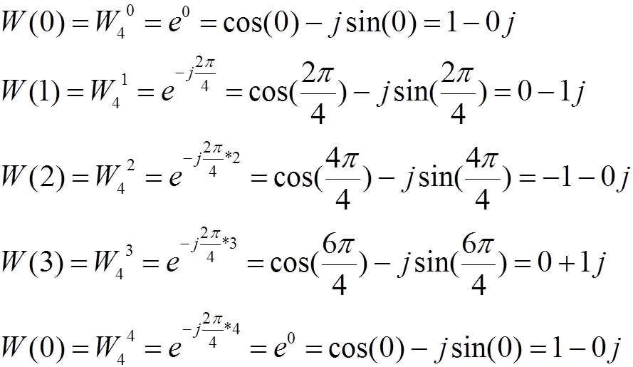
そして、W(x)は式(1)のW4のx乗に対応する。W4は式(2)で示すように2πで一周する周期関数であるので、
以下のように4種類の値がW(0), W(1), W(2), W(3)が必要となる。W(4)=W(0)となり、繰り返すことになる。
(2)FORループによる実現
式(1)を擬似Cコードで実現すると以下のようになる。
For k=0; k++; k<4
tmp = 0;
For n=0; n++; n < 4
x =n * k;
x = xの下位2ビットだけを取り出す (mod 4 と同様の処理)
y = S(n) * W(x);
tmp = tmp + y;
END
G(k) = tmp;
END
インデックスがnの内側のループでは、n*kの乗算を行い、その下位2ビットを取り出すことで、x=0から3の値を求め、W(x)により、W値をメモリから読み出し、その後入力のS値との乗算を行い、変数tmpに累積することで総和を計算している。外側のループでk値を変えることで、G(0)からG(3)の値に順に対応している。
(3)命令の追加
SRPシステムで、上記アルゴリズムに対応するために、整数の乗算命令、命令内に与えられた16ビット数値とレジスタの加算を行うaddi (Add Immediate)命令をさらに追加する。
ただし、通常32ビット数どうしを乗算すると64ビットの結果が得られるが、ここでは、64ビットの結果の内下位32ビットを結果として格納することにする。以下の表1はサポート命令で、表2はその32ビット命令の機械語の内容を各フィールドごとに10進数で示したものである。黄色い部分は、前回の講義で追加した複素乗算と複素加算命令で、水色の命令は今回追加した命令である。
表1 サポート命令
|
区分 |
命令 |
アセンブラ例 |
例の意味 |
備考 |
|
算術演算 |
add |
add R1,R2,R3 |
R1 <= R2 + R3 |
加算 |
|
subtract |
sub R1,R2,R3 |
R1 <= R2 - R3 |
減算 |
|
|
complex mul |
cmul R1, R2, R3 |
複素数R1 <=
複素数R2 * 複素数 R3 |
複素乗算 |
|
|
complex add |
cadd R1, R2, R3 |
複素数R1 <=
複素数R2 + 複素数 R3 |
複素加算 |
|
|
mul |
mul R1, R2, R3 |
R1 <= R2 * R3 |
整数乗算 ここでは、乗算結果の下位32ビットをR1に格納する。 |
|
|
addi |
addi R1, R2, 100 |
R1 <= R2 + 100 |
命令内数値とレジスタの加算 |
|
|
論理演算 |
and |
and R1,R2,R3 |
R1 <= R2 and R3 |
各ビットごとにAND |
|
or |
or R1,R2,R3 |
R1 <= R2 or R3 |
各ビットごとにOR |
|
|
データ転送 |
load word |
lw R1, 100(R2) |
R1 <= メモリ[R2+100] |
メモリからレジスタへの転送 |
|
store word |
sw R1, 100(R2) |
メモリ[R2+100] <= R1 |
レジスタからメモリへの転送 |
|
|
条件分岐 |
branch on equal |
beq R1,R2,25 |
if (R1=R2) go to PC+4+25*4 |
等しい時にPC相対分岐 |
|
set on less than |
slt R1,R2,R3 |
if (R2<R3) R1<=1 else R1<=0 |
|
|
|
無条件ジャンプ |
jump |
j 2500 |
go to 2500*4 |
絶対アドレスジャンプ |
表2 機械語フォーマット
|
区分 |
命令 |
アセンブラ例 |
形式 |
命令フォーマット(32ビット長) 各フィールドは10進数表示 |
|||||
|
6ビット |
5ビット |
5ビット |
5ビット |
5ビット |
6ビット |
||||
|
算術演算 |
add |
add R1,R2,R3 |
R |
0 |
2 |
3 |
1 |
0 |
32 |
|
subtract |
sub R1,R2,R3 |
R |
0 |
2 |
3 |
1 |
0 |
34 |
|
|
complex mul |
cmul R1, R2, R3 |
R |
0 |
2 |
3 |
1 |
0 |
48 |
|
|
complex add |
cadd R1, R2, R3 |
R |
0 |
2 |
3 |
1 |
0 |
49 |
|
|
mult |
mult R1, R2, R3 |
R |
0 |
2 |
3 |
1 |
0 |
24 |
|
|
addi |
addi R1, R2, 100 |
I |
8 |
2 |
1 |
100 |
|||
|
論理演算 |
and |
and R1,R2,R3 |
R |
0 |
2 |
3 |
1 |
0 |
36 |
|
or |
or R1,R2,R3 |
R |
0 |
2 |
3 |
1 |
0 |
37 |
|
|
データ転送 |
load word |
lw R1, 100(R2) |
I |
35 |
2 |
1 |
100 |
||
|
store word |
sw R1, 100(R2) |
I |
43 |
2 |
1 |
100 |
|||
|
条件分岐 |
branch on equal |
beq R1,R2,25 |
I |
4 |
1 |
2 |
25 |
||
|
set on less than |
slt R1,R2,R3 |
R |
0 |
2 |
3 |
1 |
0 |
42 |
|
|
無条件ジャンプ |
jump |
j 2500 |
J |
3 |
2500 |
||||
(4) アセンブラーでの実現
|
ワード番地 |
|
アセンブラーコード |
コメント |
|
0 |
|
NOP |
|
|
1 |
|
addi R10, R0, 3 |
R10 <= 3 (bit mask) |
|
2 |
|
addi R11, R0, 4 |
R11 <= 4 |
|
3 |
|
add R2, R0, R0 |
k = R2 <= 0 outer loop index |
|
4 |
LOOP1: |
add R3, R0, R0 |
tmp = R3 <= 0 |
|
5 |
|
add R4, R0, R0 |
n = R4 <= 0 inner loop index |
|
6 |
LOOP2: |
mult R5, R2, R4 |
x = R5 <= R2 * R4 |
|
7 |
|
and R5, R5, R10 |
R5 <= R5 and R10 (下位2ビット取り出し) |
|
8 |
|
mult R6, R5, R11 |
R6 <= R5(=x) * 4 |
|
9 |
|
lw R7, 288(R6) |
Load W <= MEM(288+4*x) |
|
10 |
|
mult R6, R4, R11 |
R6 <= R4(=n) * 4 |
|
11 |
|
lw R8, 256(R6) |
Load S <= MEM(256+4*n) |
|
12 |
|
cmul R9, R7, R8 |
R9 <= R7(=W) * R8(=S) (complex multiply) |
|
13 |
|
cadd R3 R3, R9 |
tmp =R3 <= R3 + R9 (complex add) |
|
14 |
|
addi R4, R4, 1 |
n++; n= R4 <= R4 + 1 |
|
15 |
|
slt R5, R4, R11 |
If(n<4) then R5<=1 else R5<=0 |
|
16 |
|
beq R5, R0, EXIT2 |
If R5=0 goto EXIT2 else next |
|
17 |
|
j LOOP2 |
|
|
18 |
EXIT2: |
mult R6, R2, R11 |
R6 <= R2(=k) * 4 |
|
19 |
|
sw R3, 272(R6) |
Store result => MEM(272+4*k) |
|
20 |
|
addi R2, R2, 1 |
k++; k=R2 <= R2 + 1 |
|
21 |
|
slt R5, R2, R11 |
If(k<4) then R5<=1 else R5<=0 |
|
22 |
|
beq R5, R0, EXIT1 |
If R5=0 goto EXIT1 else next |
|
23 |
|
j LOOP1 |
|
|
24 |
EXIT1: |
NOP |
|
(5)以下Xilinxでの実習内容
(5−1) ISEを立ち上げ、SRP_TASK0プロジェクト等をコピーして、SRP_TASK1プロジェクトを作成し、そのプロジェクトをOPEN PROJECTする。
(5−2) 2命令追加のため、OPEN でalu_pkg.vhdを拓いて、以下の赤字の追加を行い、保存を行う。
(省略)
constant OP_J : std_logic_vector
(5 downto 0)
:= "000010";
-- TSUIKA 2
constant OP_ADDI : std_logic_vector
(5 downto 0)
:= "001000";
-- function code for ADD,
SUB, SLT
constant FN_ADD : std_logic_vector
(5 downto 0)
:= "100000";
constant FN_AND : std_logic_vector
(5 downto 0)
:= "100100";
constant FN_OR : std_logic_vector
(5 downto 0)
:= "100101";
constant FN_SUB : std_logic_vector
(5 downto 0)
:= "100010";
constant FN_SLT : std_logic_vector
(5 downto 0)
:= "101001";
-- NEW INSTRUCTION
constant FN_CMUL : std_logic_vector
(5 downto 0)
:= "110000";
constant FN_CADD : std_logic_vector
(5 downto 0)
:= "110001";
-- TSUIKA 2
constant
FN_MULT : std_logic_vector
(5 downto 0)
:= "011000";
-- registers
constant R0 : std_logic_vector (4 downto 0) := "00000";(省略)
(5−3) ROMコードの中身を以下のように修正する。
(省略)
constant ROM : MemVecArr :=
(0 => OP_ALU & R0 & R0 & R0 & "00000" &
FN_ADD, -- NO operation
1 => OP_ADDI &
R0 & R10 &
"0000000000000011", -- addi R10, R0, 3
2 => OP_ADDI &
R0 & R11 & "0000000000000100", -- addi R11, R0, 4
3 => OP_ALU & R0 & R0 & R2 & "00000" &
FN_ADD, -- add R2,
R0, R0
4 => OP_ALU & R0 & R0 & R3 & "00000" &
FN_ADD, -- LOOP1: add R3, R0, R0
5 => OP_ALU & R0 & R0 & R4 & "00000" & FN_ADD, -- add R4, R0, R0
6 => OP_ALU & R2 & R4 & R5 & "00000" & FN_MULT,
-- LOOP2: mult R5, R2, R4
7 => OP_ALU & R5 & R10 & R5 & "00000" &
FN_AND, -- and R5, R5, R10
8 => OP_ALU & R5 & R11 & R6 & "00000" & FN_MULT,
-- mult R6, R5, R11
9 => OP_LW & R6 & R7 & "0000000100100000", -- lw R7, 288(R6)
10 => OP_ALU & R4 & R11 & R6 & "00000" & FN_MULT,
-- mult R6, R4, R11
11 => OP_LW & R6 & R8 & "0000000100000000", -- lw R8, 256(R6)
12 => OP_ALU & R7 & R8 & R9 & "00000" & FN_CMUL,
-- cmul R9, R7, R8
13 => OP_ALU & R3 & R9 & R3 & "00000" & FN_CADD,
-- cadd R3 R3, R9
14 => OP_ADDI & R4 & R4 & "0000000000000001", -- addi R4, R4, 1
15 => OP_ALU & R4 & R11 & R5 & "00000" & FN_SLT, -- slt R5, R4,
R11
16 => OP_BEQ & R5 & R0 & "0000000000000001", -- beq R5, R0, EXIT2
17 => OP_J &
"00000000000000000000000110", -- j
LOOP2=6
18 => OP_ALU & R2 & R11 & R6 & "00000" & FN_MULT,
-- EXIT2: mult R6, R2, R11
19 => OP_SW & R6 & R3 & "0000000100010000", -- sw R3, 272(R6)
20 => OP_ADDI & R2 & R2 & "0000000000000001", -- addi R2, R2, 1
21 => OP_ALU & R2 & R11 & R5 & "00000" & FN_SLT, -- slt R5, R2,
R11
22 => OP_BEQ & R5 & R0 & "0000000000000001", -- beq R5, R0, EXIT1
23 => OP_J &
"00000000000000000000000100", -- j
LOOP1=4
24 => OP_ALU & R0 & R0 & R0 & "00000" &
FN_ADD, -- EXIT1: NOP
25 => OP_ALU & R0 & R0 & R0 & "00000" &
FN_ADD, -- NO operation
26 => OP_ALU & R0 & R0 & R0 & "00000" &
FN_ADD, -- NO operation
27 => OP_ALU & R0 & R0 & R0 & "00000" &
FN_ADD, -- NO operation
others => OP_ALU & R0
& R0 & R0 & "00000" & FN_ADD); -- NO operation
(省略)
(5−4) RAMの内容を以下のように修正する。
(省略)
signal RAM : MemVecArr :=
(0 =>
"0000010000000000" & "0000010000000000", --MEM(256)= 1+1j
1 =>
"1111110000000000" & "1111110000000000", --MEM(260)= -1-1j
2 =>
"0000010000000000" & "0000010000000000", --MEM(264)= 1+1j
3 =>
"1111110000000000" & "1111110000000000", --MEM(268)= -1-1j
4 => conv_std_logic_vector ( 0, 32), --MEM(272)= G(0)
5 => conv_std_logic_vector
( 0, 32), --MEM(276)= G(1)
6 => conv_std_logic_vector
( 0, 32), --MEM(280)= G(2)
7 => conv_std_logic_vector
( 0, 32), --MEM(284)= G(3)
8 => "0000010000000000"
& "0000000000000000",
--MEM(288)= W(0) = 1+0j
9 => "0000000000000000"
& "1111110000000000",
--MEM(292)= W(1) = 0-1j
10 => "1111110000000000"
& "0000000000000000",
--MEM(296)= W(2) = -1+0j
11 => "0000000000000000"
& "0000010000000000",
--MEM(300)= W(3) = 0+1j
others => conv_std_logic_vector ( 0, 32) );
(省略)
(5−5) プロセッサMINIPROCのALU部分を以下のように修正する。赤字の部分が追加である。
(省略)
--------------------
--
Register File
--------------------
-- READ
operation
regout1 <= reg(conv_integer(rs));
regout2 <= reg(conv_integer(rt));
-- WRITE
operation
RFILE_WT: process (Clock)
begin
if rising_edge(Clock)
then
if (opcode = OP_ALU) and (rd /= R0)
then
reg(conv_integer(rd)) <= alu_rst;
--
TSUIKA2
elsif (opcode = OP_ADDI) and (rt /= R0) then
reg(conv_integer(rt)) <= alu_rst;
--
elsif (opcode = OP_LW) and (rt /= R0) then
reg(conv_integer(rt)) <= Rddata ;
else null;
end if;
end if;
end process RFILE_WT;
--------------------
-- ALU
-------------------
ALU_RESULT: process(opcode,
regout1, regout2, sgnexd, func)
-- TSUIKA
variable sr1 : std_logic_vector(15 downto 0);
variable si1 : std_logic_vector(15 downto 0);
variable sr2 : std_logic_vector(15 downto 0);
variable si2 : std_logic_vector(15 downto 0);
variable sr3 : std_logic_vector(15 downto 0);
variable si3 : std_logic_vector(15 downto 0);
variable tmp1 : std_logic_vector(31
downto 0);
variable tmp2 : std_logic_vector(31
downto 0);
variable tmp3 : std_logic_vector(31
downto 0);
variable tmp4 : std_logic_vector(31
downto 0);
-- TSUIKA 2
variable tmp5 : std_logic_vector(63
downto 0);
begin
if (opcode
= OP_ALU) then
if (func
= FN_ADD) then alu_rst <= regout1 + regout2;
elsif (func = FN_SUB) then alu_rst <= regout1 - regout2;
elsif (func = FN_AND) then alu_rst <= regout1 and regout2;
elsif (func = FN_OR ) then alu_rst <= regout1 or regout2;
--
TSUIKA1
elsif (func = FN_CADD) then
sr1 := regout1(31 downto
16);
si1 := regout1(15 downto
0);
sr2 := regout2(31 downto
16);
si2 := regout2(15 downto
0);
alu_rst <=
(sr1 + sr2) & (si1 + si2);
elsif (func = FN_CMUL) then
sr1 := regout1(31 downto
16);
si1 := regout1(15 downto
0);
sr2 := regout2(31 downto
16);
si2 := regout2(15 downto
0);
tmp1 := signed(sr1) * signed(sr2);
tmp2 := signed(si1) * signed(si2);
tmp3 := signed(sr1) * signed(si2);
tmp4 := signed(sr2) * signed(si1);
sr3 := tmp1(25 downto
10) - tmp2(25 downto 10);
si3 := tmp3(25 downto
10) + tmp4(25 downto 10);
alu_rst <=
sr3 & si3;
--
--
TSUIKA2
elsif (func = FN_MULT) then
tmp5 := signed(regout1) *
signed(regout2);
alu_rst <=
tmp5(31 downto 0);
--
else -- SLT
if ( regout1 < regout2 ) then alu_rst <= conv_std_logic_vector
( 1, 32);
else
alu_rst <= conv_std_logic_vector
( 0, 32);
end if;
end
if;
elsif ((opcode = OP_LW) or (opcode =
OP_SW) ) then
alu_rst
<= regout1 + sgnexd;
elsif (opcode = OP_BEQ) then alu_rst
<= regout1 - regout2;
-- TSUIKA2
elsif (opcode = OP_ADDI) then alu_rst
<= regout1 + sgnexd;
--
else
alu_rst
<= (others => '0');
end if;
end process ALU_RESULT;
ALU_ZEROFLAG: process(alu_rst) begin
if (alu_rst
= conv_std_logic_vector ( 0, 32) ) then alu_zero <= '1';
else
alu_zero <= '0';
end if;
end process ALU_ZEROFLAG;
(省略)
(5−6) シミュレーションを実行すると、以下のようになる。DRAMの中をモニターしている。
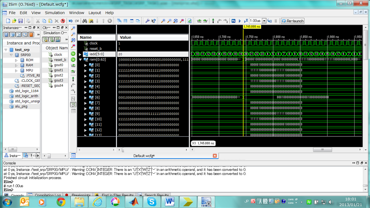
G(0)=0+0j
G(1)=0+0j
G(2)=4+4j
G(3)=0+0j
となっている。
今、入力は
S(0)=1+1j
S(1)=-1-j
S(2)=1+1j
S(3)=-1-j
であり、
であるので、
G(0)=0
G(1)=0
G(2)=4+4j
G(3)=0
であるので、正しく計算できている。
以上