Tom Wada at The University of the Ryukyus, Department of Information Engineering
This specification specifies the task to design CDMA (Code Division Multiple Access) Receiver, which is used for ,e.g., Cellar Phones. Since the design contest is intended for student level, the level of the task has to be completed is relatively low and we are trying to give attendees freedom in designing the task.
The contest needs the design using HDLs such as Verilog HDL or VHDL and, logic synthesis. Attendees do not always need to use SYNOPSYS design compiler. Instead, other synthesis tools such as tools for FPGA are also welcome.
If attendees have extra capability, it is recommended to make real FPGA or other form of implementation. This extra work will be reasonably evaluated in the contest.
Let's start the explanation of the task "Digital CDMA Receiver".
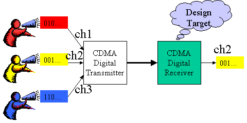
Figure 1 CDMA communication system
The figure 1 shows an example of CDMA communication system. It consists of Transmitter and Receiver. The task to design in the contest is Only "Receiver". The transmitter receives 3 digital inputs, and then it mixes the 3 data to generate one output. The method of the mixture is CDMA. Receiver receives the mixture, and then it decodes the signal and extracts one preferable datum.
Although in a real communication system, the output of the transmitter (base-band signal) will be converted to higher frequency pass-band signal by the "mixer", for the simplicity such a mixer is not used in the design task.
Since usually the transmitter and the receiver are physically isolated, the common CLOCK signal is not available. But in this design task, we assume the perfect synchronized CLOCK for both the transmitter and the receiver.
CDMA is not so easy method. But this specification try to explain how to design "the CDMA receiver" as easy as possible intending the audiences do NOT have previous knowledge of CDMA. If you have the knowledge of the digital design and skill of HDL, please feel free to try the task.
CDMA stands for Code Division Multiple Access. The Multiple Access means that plural data is convoyed using one transmitting channel. Please take a look at the figure 1. The thick line with arrow is the transmitting channel, and three data is transmitted via the channel.
The receiver has to extract wanted datum from the data mixture in the channel. CDMA does this data extraction using Pseudo Noise Code (PN code). The PN code is the sequence consisting of randomly appearing ones and zeros, but the appearing frequency of both ones and zeros are almost same.
Using the PN code that has length of 7, the characteristics of PN code will be explained as follows.
Assume the following PN code.
| ÇP | ÇP | ÇP | ÇO | ÇP | ÇO | ÇO |
The PN code is plotted in time as figure 2.

Figure 2 Time plot of the PN code
Let's compare the PN code with time-shifted PN code. Figure 3 shows the original PN code and the time-shifted PN code. The time difference is "2".
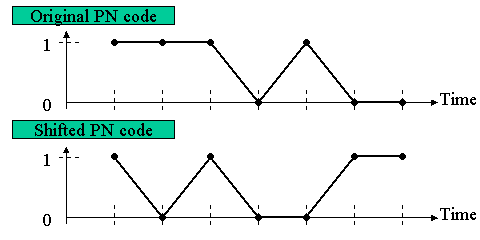
Figure 3 Comparison between the PN code and the time-shifted PN code
How these two codes are similar? The similarity of two waves can be evaluated using "correlation". The definition of the correlation is as follows.
Correlation = how many times the codes are same - how many times the codes are different
The correlation value of the figure 3 is '-1' , and then the value is close to '0'. This means those two waves are NOT similar or orthogonal. The following table summarizes the correlation values. The values at time-shift=0, time-shift=7, which means the two waves are perfectly match, are the maximum value '7'. The other values are all '-1', close to zero.
| Time-shift | PN code | the number of "same" | the number of "difference" | correlation value | ||||||
| 0 | 1 | 1 | 1 | 0 | 1 | 0 | 0 | 7 | 0 | 7 |
| 1 | 1 | 1 | 0 | 1 | 0 | 0 | 1 | 3 | 4 | -1 |
| 2 | 1 | 0 | 1 | 0 | 0 | 1 | 1 | 3 | 4 | -1 |
| 3 | 0 | 1 | 0 | 0 | 1 | 1 | 1 | 3 | 4 | -1 |
| 4 | 1 | 0 | 0 | 1 | 1 | 1 | 0 | 3 | 4 | -1 |
| 5 | 0 | 0 | 1 | 1 | 1 | 0 | 1 | 3 | 4 | -1 |
| 6 | 0 | 1 | 1 | 1 | 0 | 1 | 0 | 3 | 4 | -1 |
| 7 | 1 | 1 | 1 | 0 | 1 | 0 | 0 | 7 | 0 | 7 |
Next, let's consider the correlation between the PN code and the inverted PN code. The figure 4 shows both codes.
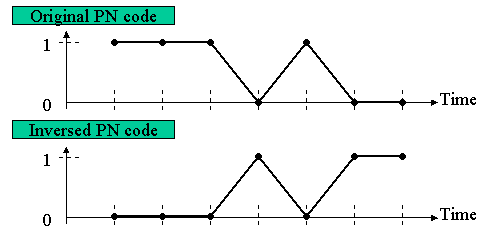
Figure 4 Comparison between the PN code and the Inverted PN code
Since the code is inverted, the correlation value is '-7', that is negative large value.
According to the explained characteristics, the following data transmitting and reception are possible.
For 1 bit data-A transfer, if data-A= '0' is transferred, send the original PN code (PN1). If data-A= '1' is transferred, send the inverted PN code (Inverted PN1).
Simultaneously, another 1 bit data-B can be transferred on the same channel using the time-shifted PN code (PN2) as follows.
If data-B= '0' is transferred, send the PN2 code. If data-B= '1' is transferred, send the inverted PN2 code.
On the channel, these plural codes are added.
At the receiver, the correlation between the PN1 code and the added signal gives the correlation between the PN1 code and data-A's PN code since the correlation between PN1 and PN2 is close to zero.
Then the, if the correlation at the receiver is large positive value, the data-A can be identified as '0'. Instead, if it is large negative value, the data-A can be identified as '1'.
In the next section, another example will be described.
The simple example which PN code length is '7' is described as follows.
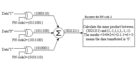
Figure 5 Simple CDMA communication system
The figure shows the system that is using 3 PN codes and is sending 3 data.
PN code1 = {0111001} for data "1"
PN code2 = {1011100} for data "0"
PN code3 = {0101110} for data "1"
Each PN code is exclusive ORed with corresponding data, and then is summed up to generate the output sequence of {3021211}.
At the receiver, the sequence of {3021211} is received, and then the correlation value with PN code 2 is calculated. The actual calculation performed at the receiver is the vector's inner product between the code {3021211} and the code {1,-1,1,1,1,-1,-1}. The latter code {1,-1,1,1,1,-1,-1} is the modified PN code2, in which '0' is converted to '-1'.
If the result is large positive value, the data sent using the PN code 2 identified as '1'. Instead, if the result is large negative value , the data sent using the PN code 2 will be '1'.
Then the receiver has to perform the inner product calculation. This calculation is also called as "convolution" or "matched filtering".
NOTE:
In the above example, the PN code length of 7 is used. But since the code length is very short, it has been observed that clear correlation results might not obtained by the inner product calculation.
Then, the actual design task uses the code length of 127. Be sure to remember!
The target sytem is shown in the figure 6. The system is organized by the transmitter and the receiver. Design task is just the receiver. The HDL code (sorry! VHDL only) for the transmitter will be given later.
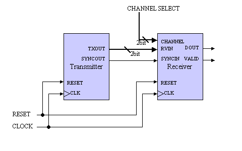
Figure 6 System Organization
The transmitter includes 3 kinds of PN code generators (for channel 1, channel 2, and channel 3), 3 kinds of sending data generator, and 3 exor gates for each transmitting channel. As explained in the section of [2] One example of CDMA communication system, each PN generator output is exclusive ORed with the corresponding sending datum, and then those signals are summed up to generate 2 bits width TXOUT output signal.
The TXOUT signal is generated synchronizing with the CLOCK rising edge. Since the length of the PN code is 127, it takes 127 cycle to send 1 bit datum on each channel. In order to indicate the timing of the PN code starting point, the synchronizing signal SYNCOUT is asserted.
The HDL of the transmitter and its test bench (sorry, VHDL only) is given as follows. The sending data are the repeat of {01010101} for channel1 (CH1), {00110011} for CH2, {00001111} for CH3.
VHDL for transmitter : transmitter.vhd
VHDL for the test bench : test_tx.vhd
The receiver gets the 2 bits input RVIN from the transmitter's TXOUT. Since the signal RVIN is composed by the mixture of CH1, CH2, and CH3 sending data, preferred channel data has to be extracted from the RVIN signal according to the 2 bits width CHANNEL inputs. Then the extracted data will be output to the DOUT pin. CHANNEL="00" is don't care, "01" corresponds CH1, "10" corresponds CH2, and "11" corresponds CH3.
By the assertion of the SYNCIN signal, the receiver can know the start point of the PN code. From this starting point, 127 data are received and the inner product calculation with the PN code, which is generated in the receiver according to the CHANNEL input, is calculated. If the result of the inner product is large positive value, the sending datum is identified as '0' and if it is large negative value , the sending datum is identified as '1'.
In the design task, the judgement of the inner product size is 40. If the inner product > 40, the OUT is '0' and if the inner product <-40, the DOUT is '1'.
The pin assignment of the transmitter and the receiver are shown in the Table 1.
| Transmitter | Å@ | Receiver | ||||||
| Signal | IN or OUT | Bit width | Description | Å@ | Signal | IN or OUT | Bit width | Description |
| CLK | IN | 1 | clock | Å@ | CLK | IN | 1 | clock |
| RESET | IN | 1 | reset at '1' | Å@ | RESET | IN | 1 | reset at '1' |
| TXOUT | OUT | 2 | sending data | Å@ | RVIN | IN | 2 | receiving data |
| SYNCOUT | OUT | 1 | synchronize signal | Å@ | SYNCIN | IN | 1 | synchronize signal |
| Å@ | Å@ | Å@ | Å@ | Å@ | CHANNEL | IN | 2 | channel selection 00: DONT' CARE 01: CH1 10: CH2 11: CH3 |
| Å@ | Å@ | Å@ | Å@ | Å@ | DOUT | OUT | 1 | data output |
| Å@ | Å@ | Å@ | Å@ | Å@ | VALID | OUT | 1 | '1' when DOUT is valid |
Table 1 Pin assignment for standard level task
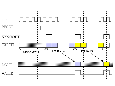
Figure 7 Operation waveform
Figure 7 shows the operation waveform of the system. After the de-assertion of RESET, the transmitter outputs TXOUT signal. It takes 127 cycle to send 1 bit data on each channel. SYNCOUT signal is also asserted as shown in the figure to indicate the starting point of the 127-length data set.
The receiver does calculate the inner product. For example,
Assume the
RVIN input sequence as follows,
{3, 0, 1, 2, 0 ,3, 1, 1, 2, 3, 2, 1, 0, 1, 2, ...}
Assume the
PN code for the receiving channel as follows,
{1, 1, 1, 1, 1, 1, 1, 0, 1, 1, 1, 0, 1, 1, 0, ...}
Then the
inner product calculation will be as follows ('0' in the
PN code is converted to '-1'),
Inner product = 3+0+1+2+0+3+1-1+2+3+2-1+0+1-2+...
If the inner product > 40, DOUT becomes '0' and VALID is '1'. If the inner product < -40, DOUT becomes '1' and VALID is '1'. If 40 >= the inner product >= -40, VALID becomes '0' and DOUT is '0' or HiZ.
The PN codes used in the design task is given as follows. The lengths of all code are 127.
In addition, all these PN codes can be generated by linear feedback shift registers. The corresponding circuit schematic will be shown as follows. Be sure to remember that the initial conditions of all D-type flip-flops are '1'.
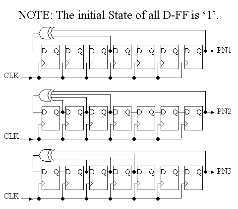
Figure 8 127-length PN code generators
If you think the design task is too complicated, you can remove CHANNEL input from the receiver. Then the receiver only receives the data on channel 1 (CH1). The corresponding pin assignment is shown in Table 2.
| Receiver | |||
| Signal | IN or OUT | Bit width | description |
| CLK | IN | 1 | clock |
| RESET | IN | 1 | reset at '1' |
| RVIN | IN | 2 | receiving data |
| SYNCIN | IN | 1 | synchronize signal |
| DOUT | OUT | 1 | data output |
| VALID | OUT | 1 | '1' when DOUT is valid |
Table 2 Pin assignment for beginners' task
In the standard level design task, the synchronizing signal is given. Then the design is somehow straightforward. For the advanced students, the receiver , which does NOT have the synchronization signal input, is prepared. The pin assignment for advanced design task is shown in Table 3.
Since the starting point of the PN code is unknown, the receiver has to find out the starting point by the following decision. Once the synchronization is accomplished, every 127 cycles VALID will become '1'.
| Receiver | |||
| Signal | IN or OUT | Bit width | description |
| CLK | IN | 1 | clock |
| RESET | IN | 1 | reset at '1' |
| RVIN | IN | 2 | receiving data |
| CHANNEL | IN | 2 | channel selection 00: DONT' CARE 01: CH1 10: CH2 11: CH3 |
| DOUT | OUT | 1 | data output |
| VALID | OUT | 1 | '1' when DOUT is valid |
Table 3 Pin assignment for the advanced design task
If you think other modification of the spec will be interesting and appeal for contest judges, further spec modification is welcome. Please explain why you did the modification in the report.
Since it is impossible to use the same synthesis library for various participants, use the 1 exor gate delay as a unit for speed comparison.
In the previous example, total delay = 7.17 ns and 6 circuit stages, then the 7.17/6= 1.195 ns is the unit of the speed. Please normalize your circuit speed by this unit.
| Title page | 1 | Team name, Members Name, School, Grade |
| 2 | Address, Phone, Email-address | |
| 3 | T-shirt size for all members in the team | |
| 4 | Which level of task is designed. | |
| Contents | 1 | Circuit block or architecture description |
| 2 | Designed circuit functional explanation, etc. | |
| 3 | Appealing point and originality | |
| 4 | Critical path speed, and circuit area | |
| 5 | HDL codes (VHDL or Verilog HDL) | |
| 6 | Simulation waveform indicating the design is operating! | |
| 7 | Anything you want to claim |
Report has to be emailed to the following address. Please use PDF file format.
If you want to send the report data other than PDF, please consult me.
ENJOY HDL! We want to see you at OKINAWA!